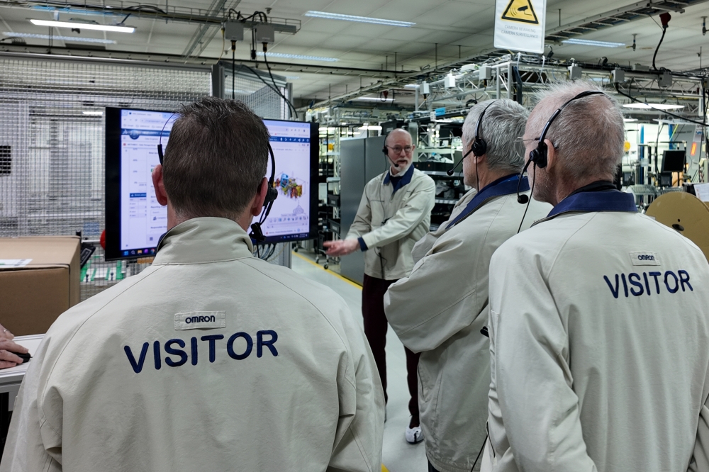
New wafer inspection and metrology platform from TRI
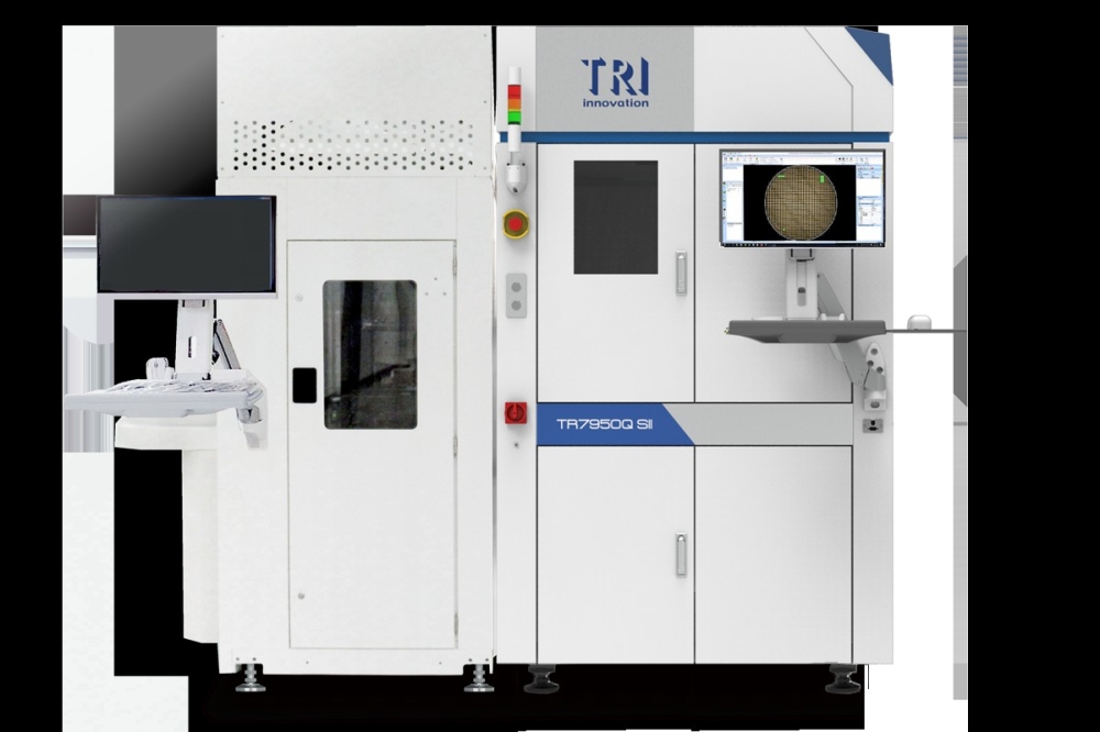
Test Research, Inc. (TRI), provider of Test and Inspection solutions for the electronics manufacturing industry, is launching the TR7950Q SII Series.
This highly modular platform is a dedicated solution for Back End Process and Advanced Packaging Inspection, ranging from patterning to wafer saw, and is engineered to set new benchmarks in wafer inspection and micro-measurement metrology.
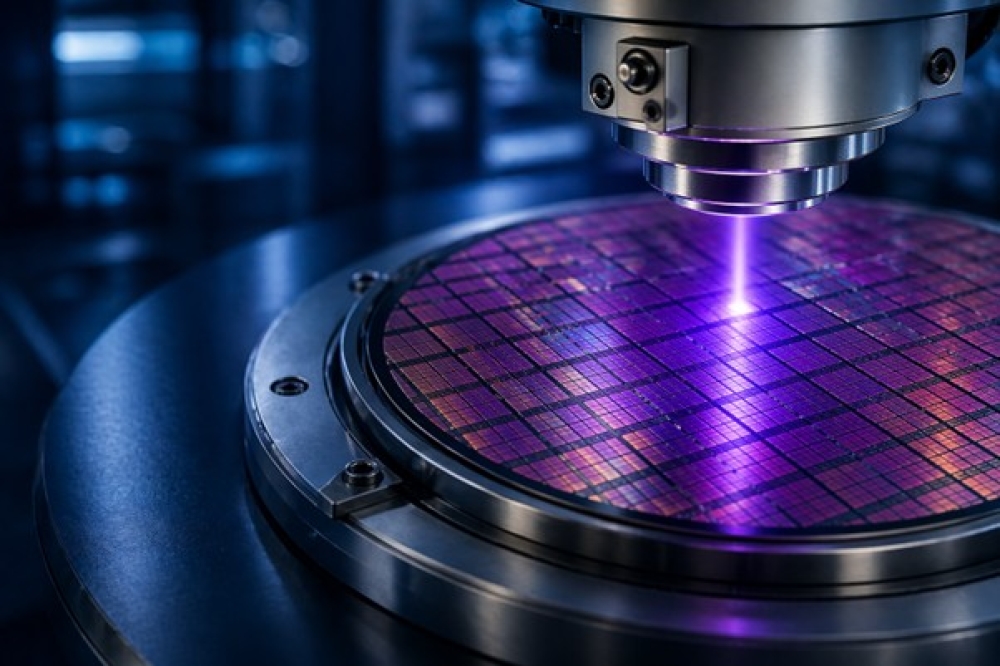
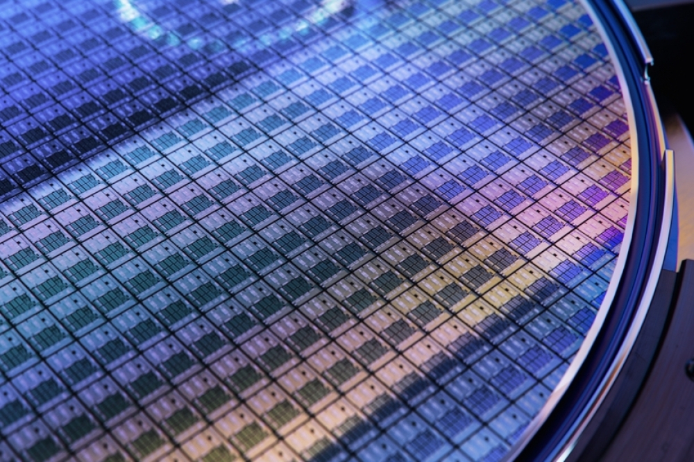
The AI-powered Wafer Metrology and Inspection Platform, TR7950Q SII, is built on a high-stability granite platform and the system supports 6" to 12" wafers. The platform features robust Automated Visual Inspection (AVI) for high-speed detection of surface defects, including particles, scratches, chipping, contamination, and foreign materials.
The optional Short-Wave Infrared (SWIR) module allows the system to penetrate silicon to detect hidden inner cracks and subsurface defects invisible to standard sensors. For high-detail requirements, the platform offers 0.5 µm or 1 µm high-resolution imaging via the 3D DFF (Depth from Focus) module.
The TR7950Q SII provides high-precision metrology for wafer thickness, top-side warpage, and complex surface topography, alongside high-speed sensing for Through-Silicon Via (TSV) depth, trench dimensions, thin film, and Chiplet metrology.