Synopsys launches multiphysics solutions
New platform integrates multiphysics analysis across chip, package and photonic design workflows to support advanced semiconductor and multi-die systems.
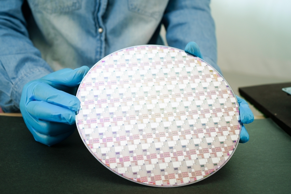
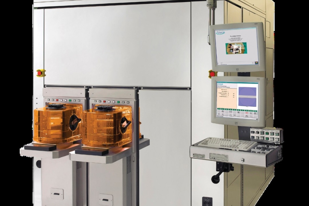
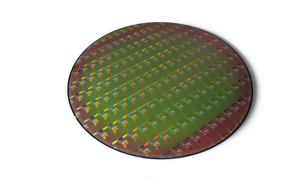
Synopsys has announced the availability of the first wave of its Multiphysics Fusion solutions, designed to help semiconductor companies address the growing complexity of advanced chip, packaging and photonic system design.
The portfolio combines Synopsys' AI-powered electronic design automation (EDA) tools with Ansys signoff technologies, enabling engineers to incorporate power, thermal, electromagnetic and signal integrity effects directly into design workflows.
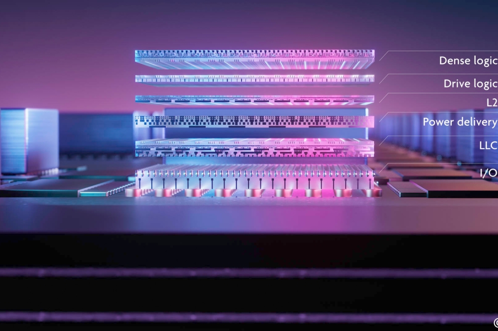
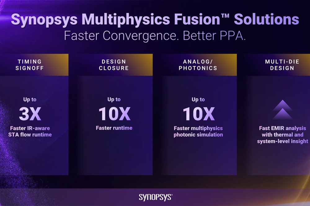
The initial release includes solutions for timing signoff, design closure, multi-die integration, and analog and photonic design. Synopsys said the platform enables concurrent analysis across silicon, packaging and optical domains, helping engineers identify issues earlier and reduce costly design iterations.
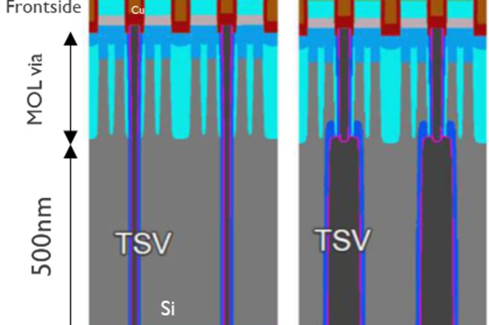
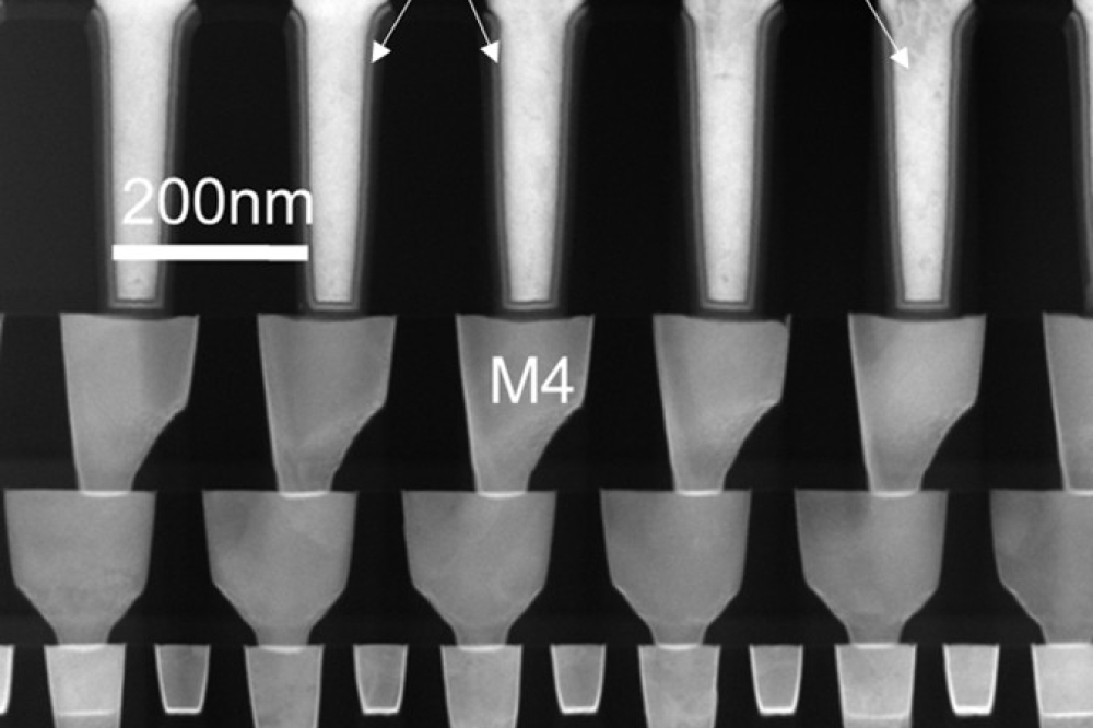
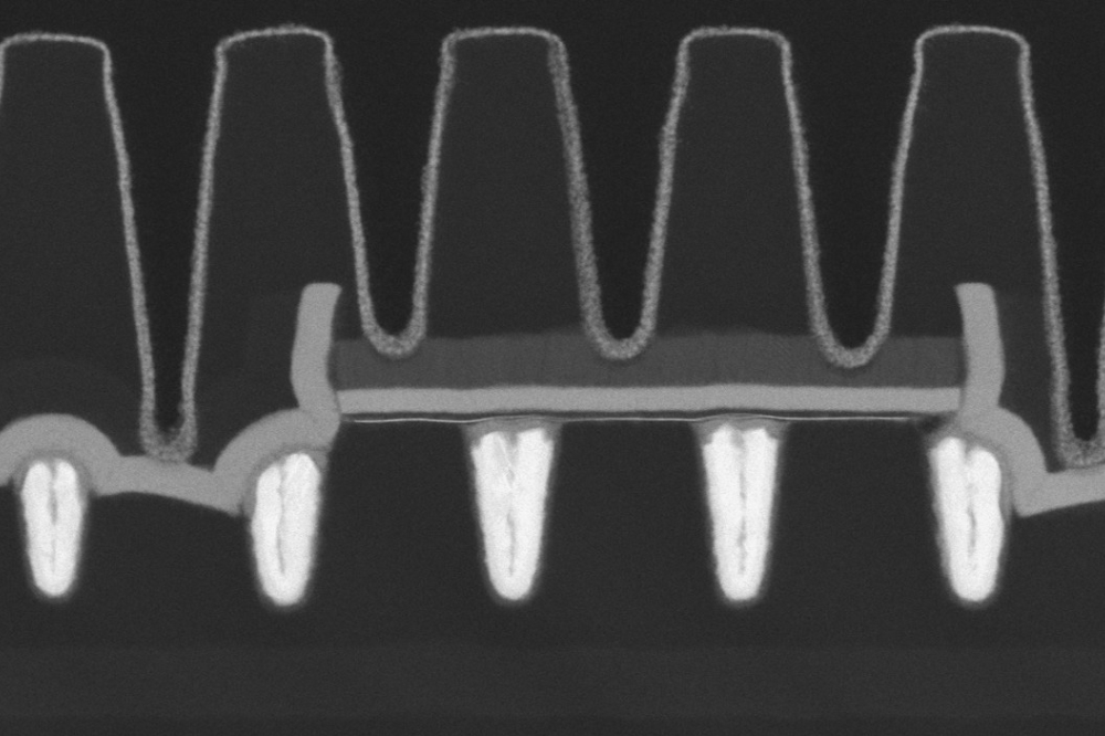
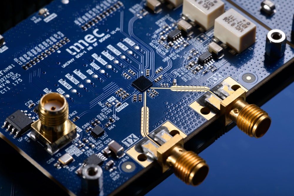
For advanced packaging applications, the Multiphysics Fusion for Multi-die Designs solution integrates power integrity, thermal and electromagnetic analysis within a unified workflow, providing system-level visibility from design exploration through to signoff.
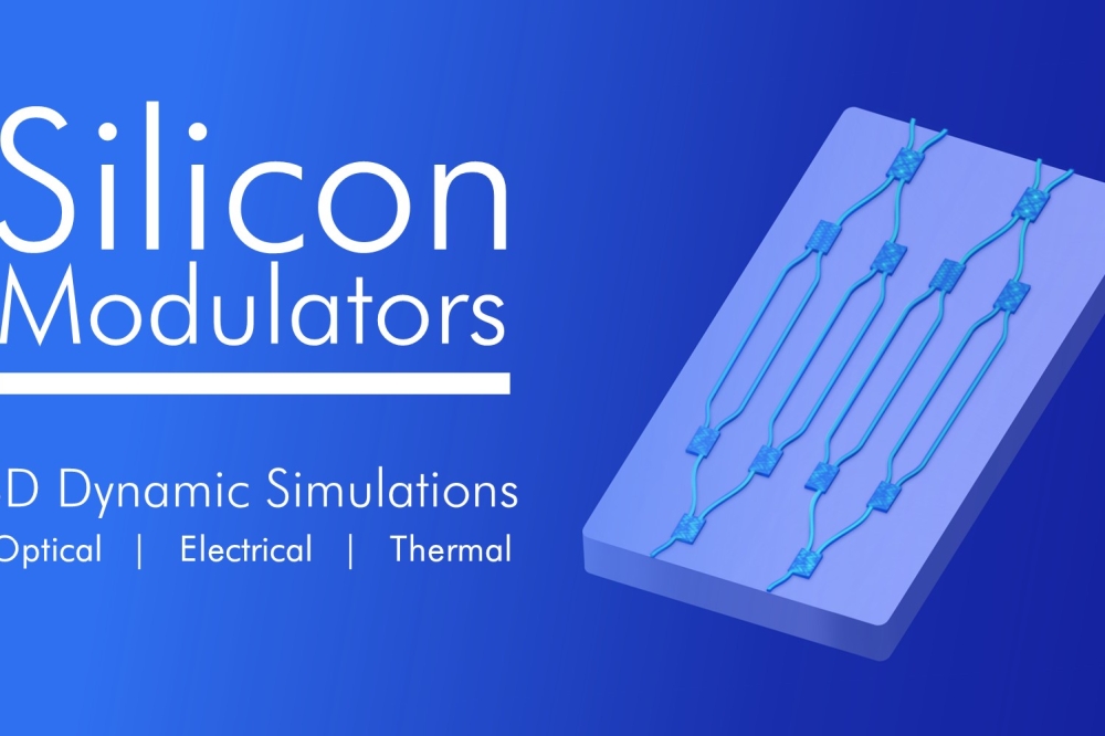
The company also highlighted support for photonic integrated circuits and co-packaged optics through the integration of OptoCompiler and Lumerical technologies, enabling end-to-end photonic and electronic co-design.
Industry partners including MediaTek, NVIDIA, Samsung Foundry and Cisco have participated in early deployments of the platform, with Synopsys reporting improvements in design closure times, runtime performance and signoff accuracy.
The launch reflects increasing industry demand for tools capable of managing the interactions between silicon, advanced packaging and optical technologies as AI and high-performance computing systems become more complex.