Bringing grayscale lithography closer to production reality

As demand grows across micro-optics, MEMS and advanced surface engineering, traditional lithography approaches are being stretched. Built around binary exposure, they can limit how efficiently engineers create depth and profile, often requiring multiple process steps to achieve the desired result.
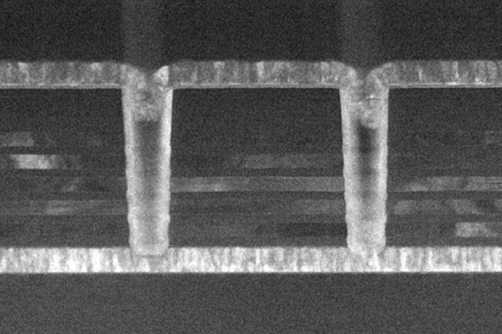
Grayscale lithography offers a different approach. By enabling controlled variation in exposure and development, it allows engineers to define height, depth and surface profile within a single resist layer. The result is greater design freedom, fewer process stages and improved efficiency in applications where geometry directly influences performance.
Despite this, adoption has remained relatively limited, often due to uncertainty around how grayscale behaves in practice and where it adds the most value.
“Grayscale lithography isn’t just about what’s possible, it’s about what’s practical,” says Dr David Shaw, Business Manager at A-Gas Electronic Materials. “Our role is to help customers understand where it fits, how it behaves in real processes, and how to apply it with confidence.”
mr-P 22G is designed to support advanced 3D microfabrication, enabling ultra-thick film applications and deep, high-resolution patterning within a single process step. This makes it particularly suited to applications such as micro-optics, MEMS and MOEMS, where precise surface geometry is critical to performance.
With only a limited number of true grayscale resists available, it provides engineers with a practical option for moving beyond conventional lithography constraints and exploring more complex structures.
A-Gas Electronic Materials is supporting adoption through material selection, process guidance and technical troubleshooting, helping customers bridge the gap between material capability and real-world process performance.