ZEISS opens Semiconductor Innovation Center in Korea
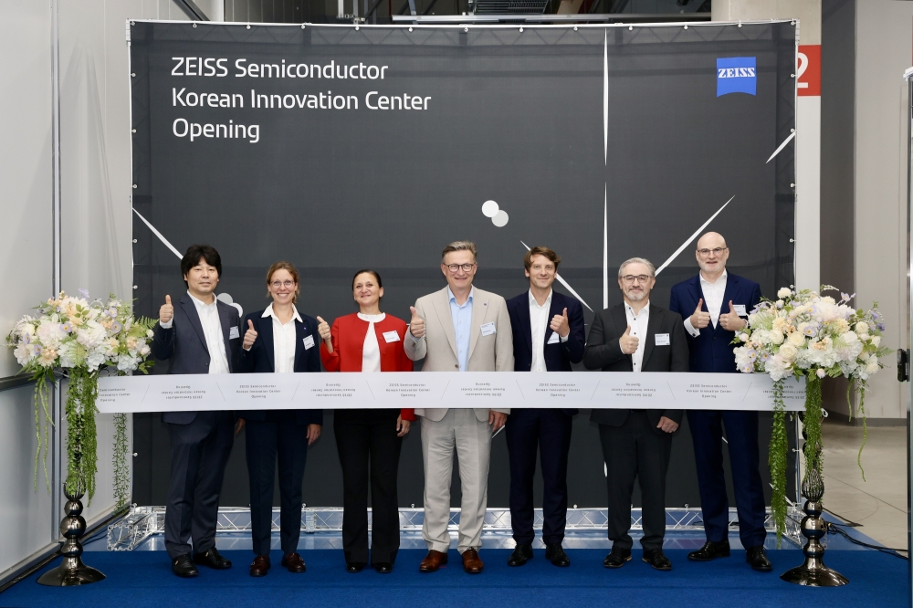
New ZEISS Semiconductor Innovation Center in Yongin strengthens the company’s presence in one of the world’s key semiconductor markets, creating a platform to bring ZEISS closer to leading chip and mask manufacturers in Korea.
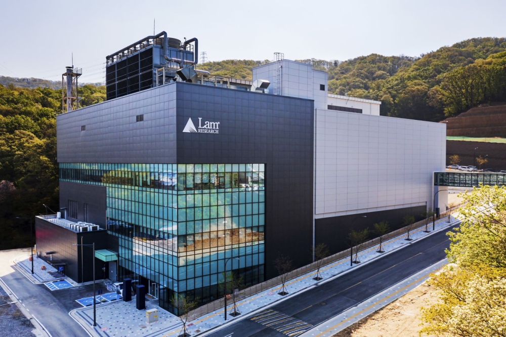
ZEISS Semiconductor Manufacturing Technology (SMT) has opened a new ZEISS Innovation Center in Yongin, Korea. With this step, ZEISS is expanding its footprint in one of the world’s most important semiconductor markets and strengthening its global network of locations supporting the industry.
The opening ceremony was attended by Dr. Frank Rohmund, President & CEO of ZEISS Semiconductor Manufacturing Technology and Member of the ZEISS Executive Board, Dr. Thomas Stammler, Chief Technology Officer, Dr. Karoline Piegdon, Head of Semiconductor Fab Solutions (SFS), Dr. Clemens Neuenhahn, Head of Semiconductor Mask Solutions (SMS), and Dr. Jaane Seehusen, who will be appointed Head of ZEISS South Korea as of September 1, 2026, as well as representatives from the Korean semiconductor industry and the German Embassy in Korea, the European Union Chamber of Commerce Korea, and the Korean-German Chamber of Commerce and Industry.
Local access to ZEISS solutions for high-volume wafer production and advanced packaging
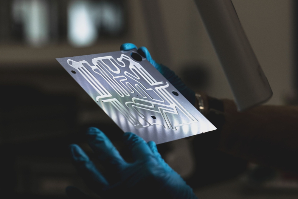
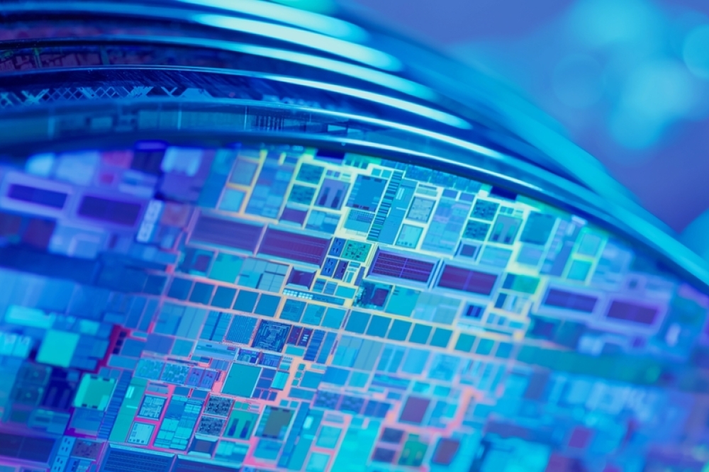
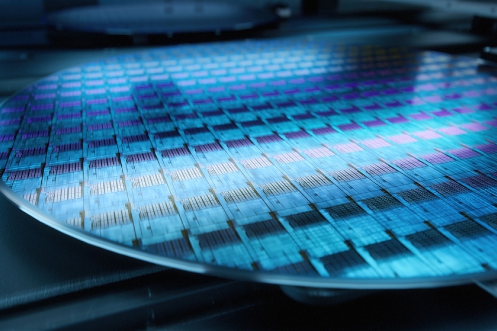
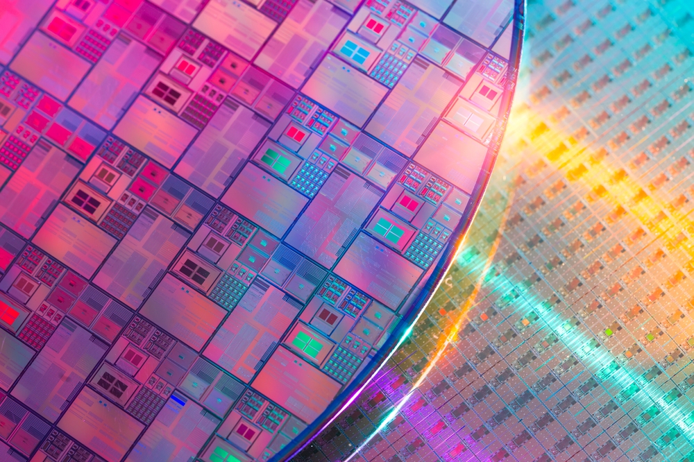
At the new Innovation Center, ZEISS brings together selected systems and solutions from its Semiconductor Mask Solutions and Semiconductor Fab Solutions portfolios. The center is designed to support innovation in high-volume wafer production and advanced packaging applications by leveraging high-precision metrology and inspection, and mask repair technologies.
The systems installed include:
NLX-100: a 3D X-ray metrology & inspection solution that provides high-resolution X-ray diagnostics and data on complex package structures and supports process control, for example in wafer-level and advanced packaging.
DUNE 100: enables active wafer shape control with integrated, high precision metrology, allowing fabs to measure and correct global wafer warpage individually for each wafer at every critical step.
MeRiT AE: a future next-generation mask repair technology. It will further extend the capability to repair the most critical and smallest defects on photomasks, with a continued high yield, which is crucial for fine advanced semiconductor processes.
In the future, ZEISS intends to install additional solution equipment in the Korean Innovation Center to strengthen early technical cooperation with customers in Korea.
Local hub for customer collaboration
The ZEISS Semiconductor Innovation Center in Korea functions as a collaborative platform for direct engagement with Korean leading chip manufacturing customers. Dr. Frank Rohmund said, "We are pleased to open our first global Semiconductor Innovation Center in Korea, as one of the key locations for the global chip industry. With this center we are moving ZEISS closer to our customers. We want to be a reliable, long term partner for our customers in Korea and further deepen our collaborations."
By enabling on-site development, process optimization and faster qualification for high-volume production environments, the center helps to accelerate the transition from research and development to customer adoption.
Dr. Jaane Seehusen, future Head of ZEISS Korea, states: “The Innovation Center in Yongin is an important step in our strategy to strengthen customer interaction in the semiconductor industry and additionally ZEISS‘s overall presence in Korea.”