Applied Materials launches deposition and etch systems for 3D chip scaling

Applied Materials has introduced two semiconductor manufacturing systems designed to enable precision processing in the increasingly deep and narrow 3D structures used in advanced logic and memory devices
Applied Materials has introduced two chip making systems aimed at processing the increasingly deep and narrow 3D structures used in advanced logic and memory devices.
The company, which supplies materials engineering technology to the semiconductor industry, said the new deposition and etch tools would help chip makers extend scaling in logic and memory, delivering higher performance, better energy efficiency and improved manufacturing yield for next-generation AI chips.
Rising demand for AI compute is speeding the industry's move to advanced 3D device architectures, including gate-all-around (GAA) transistors and high-layer-count 3D NAND. As features grow deeper and narrower in these vertical structures, conventional deposition and etch processes struggle to spread materials evenly from top to bottom, producing variability that can weaken electrical performance and cut yield.
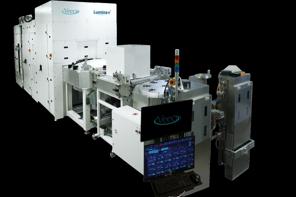
To tackle this, Applied is launching Centris Spectral SiN ALD (atomic layer deposition) and Producer Selectra Mo Etch. The company said the two systems give chipmakers precise control over both dielectric film deposition and metal removal in high-aspect-ratio structures, allowing more uniform materials engineering at advanced nodes and continued 3D scaling with tighter process control and better manufacturability across logic and memory.
Dr Prabu Raja, president of the Semiconductor Products Group at Applied Materials, said that as the industry pushed the limits of AI computing, the biggest opportunities were increasingly in materials engineering. From transistor structures to memory stacks, he said, chipmakers needed new ways to deposit and selectively remove materials precisely in complex 3D architectures. He said the latest systems offered differentiated capabilities to help customers overcome scaling barriers and accelerate innovation in logic and memory.
Uniform deposition in demanding 3D structures
Silicon nitride (SiN) is a foundational material for several chipmaking steps, including surface passivation, dielectric isolation and the creation of patterning spacers. The films must be deposited at low temperature to protect neighbouring features and be chemically robust enough to survive aggressive downstream processing.
Conventional plasma-enhanced deposition cannot uniformly treat the high-aspect-ratio structures in advanced 3D chips, resulting in poor-quality SiN films. Centris Spectral SiN ALD addresses this with a high-density microwave plasma technology that deposits high-quality SiN inside tall, narrow structures, removing the trade-off between plasma density and ion-induced damage seen in conventional approaches. The system enables dense, uniform SiN deposition at low temperatures, even in difficult 3D structures.
The tool has several applications supporting continued scaling in both DRAM and logic. In GAA transistors, for example, it can form high-quality liners for transistor contacts that reduce resistance and capacitance at critical interfaces, enabling faster performance.
Centris Spectral SiN ALD is the latest system based on Applied's Spectral ALD platform, a series of ALD tools featuring a quad reactor design with precise chemical delivery, a range of plasma and thermal processing capabilities, and hardware for both temporal and spatial ALD operation, allowing a broad range of advanced films for AI chips. The company said leading chipmakers were adopting the system.
Selective metal removal for 3D NAND
As 3D NAND scales to higher layer counts, new metal integration steps are pushing conventional patterning methods beyond their limits. Low-resistance metals such as molybdenum (Mo) are being adopted for wordline metallisation, which requires precise isolation between individual wordlines to prevent electrical shorts and reduce unwanted capacitance. Wet etch has traditionally separated wordlines, but in today's tall 3D stacks liquid chemistries struggle to reach the full depth of high-aspect-ratio features, producing top-heavy etch profiles that limit performance, yield and scalability.
Producer Selectra Mo Etch introduces highly selective metal removal, enabling precise, uniform wordline separation across the full stack. Using engineered process control and advanced gas delivery, the system overcomes wet etch limitations to deliver better top-to-bottom uniformity and tight profile precision in deep features.
By reducing cell-to-cell variability in the 3D NAND stack, the system helps lower leakage and improve data retention. Applied said the tool, already validated in high-volume manufacturing, set a new benchmark for selective metal etch and enabled a move away from legacy wet processes for continued scaling of next-generation 3D NAND. The system extends the Selectra range beyond dielectric and silicon applications into advanced metal integration, with new opportunities across NAND, DRAM and foundry-logic.
Showcase at the 2026 VLSI Symposium
Applied is presenting the systems alongside the 2026 IEEE Symposium on VLSI Technology and Circuits, where the industry is meeting to discuss developments shaping AI-driven semiconductor innovation. During the conference, on 16 June, Applied is also hosting a panel discussion on how system architectures, logic and memory technologies, advanced packaging and manufacturing must evolve and co-optimise to support the next wave of AI-driven compute.