
News Article
NXP Semiconductors Unveils Tiniest Ever CMOS Logic Package
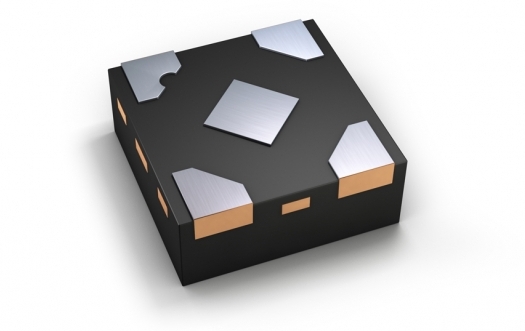
The firm's large pad pitch "Diamond" package is claimed to solve critical space issues in the design of mobile devices
NXP Semiconductors is marketing the new SOT1226 "Diamond" chip.
The firm claims this is the world's smallest general-purpose logic package, featuring a unique pad pitch design.
The SOT1226 comes in a compact 0.8 x 0.8 x 0.35 mm leadless plastic package and is 25 percent smaller than the SOT1115, which NXP boasts was previously the world's smallest logic package. The5 lead package in the new module comes with general-purpose Low Voltage CMOS and Advanced Ultra-low Power CMOS logic functions.
Despite its smaller package size, the SOT1226 can save engineers time and costs by offering a 0.5-mm pad pitch that is 50-percent larger for easier soldering. Ideally suited for portable devices such as smartphones where PCB space is critical, the unique form factor of the Diamond package enables device miniaturisation by offering a space-saving logic solution without the added manufacturing costs associated with smaller pad pitch patterns.
Typical manufacturing processes for packages use a small 0.3-mm or 0.35-mm pad pitch, requiring Electronic Manufacturing Services and assembly houses to use a step-down mask in order to successfully mount the devices on the PCB. Due to the Diamond package's larger 0.5-mm pad pitch, a step-down mask is not needed during the soldering process, saving costs for the manufacturer.
What's more, the larger pad pitch of the Diamond package offers a larger contact area, resulting in easier component placement, and improved joint strength and robustness, while reducing the risk of short circuits. With larger pad pitches, NXP says PCB assemblers can avoid costly mistakes such as solder bridging, or the formation of accidental bridges between contacts, which can render electrical devices useless.
"Mobile designers are constantly faced with the challenge of adding more functionality and features into portable devices while using less space, which in turn introduces new challenges," says Kristopher Keuser, director of marketing, Logic business line, NXP Semiconductors.
"NXP's new Diamond package is a game-changing solution that allows our customers to design within smaller geometries without increasing manufacturing costs, and to standardise their entire product portfolio. It underscores our commitment to leadership, innovation and understanding of a market that is driven by the need for smaller, cheaper and more reliable solutions."
NXP's logic business started off as Signetics fifty years ago, and then evolved into Philips Semiconductors. The firm says it's devices can support the highest volume logic requirements while offering a broad variety of package solutions.
Samples of the SOT1226 are already shipping to customers and will be available for volume shipping in June 2012.


