
3-D Solder Paste Inspection Does More Than Defect Detection
In SMT electronic assembly production, 3-D SPI has established
itself as the additional inspection gate to complement optical or X-ray
inspection.
The key task is detecting printed pads in terms of volume, form, smearing and offset. Apart from defect detection, Viscom says its 3-D SPI can accomplish much more.
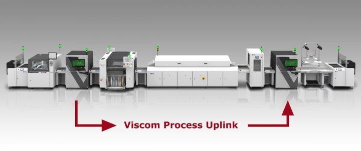
The SPI-AOI-Uplink function links paste inspection and post-reflow inspection results for both easy and effective process control as well as improved classification of AOI results.
The 3-D solder paste detects defects in paste print. Electronic assemblies that do not meet the specified criteria are sorted after the solder paste is printed. Viscom claims this is why the 3-D SPI saves the unnecessary costs of reworking electronic assemblies, particularly in high quality electronic products.
The Viscom S3088 SPI quickly performs these tasks reliably and the combination of basic AOI technology alongside high performance 3-D SPI sensor technology results in an efficient inspection process. All essential 3-D features such as volume, height and form are recorded and checked, as well as surface area, displacement and smearing.
To detect solder paste defects, generally only a deviation of
about ±50 percent from the target value is necessary to find all relevant
defects. The SPI system has a significantly higher measuring accuracy and the
typical irregularities inherent in the paste print process prohibit tighter
tolerance thresholds.
Viscom says its SPI system provides far more accurate measurement data about the solder paste than other systems, and the data obtained can be used to improve process quality and fully exploit the performance capacity of 3-D solder paste inspection. Touted as "Viscom Process Uplink", the data from the SPI and the post-reflow AOI are linked and transferred to the verification station after the AOI.
Advantages of the system are an easier classification and prevention of human error and false calls by display of the AOI-SPI defect image pairs. Secondly, higher product quality is possible through the additional display of SPI borderline defects at the AOI verification station. As a rule, borderline defects do not result in optimum solder quality. Finally, the tool offers direct process monitoring and improvement regarding paste print and solder defects.


