
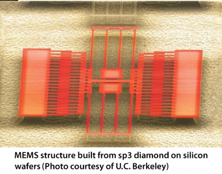
UC Berkeley Selects sp3 Reactor To Grow Diamond-On-Silicon For MEMS
sp3 Diamond Technologies, Inc., has shipped its Model 655D Series hot filament CVD diamond reactor to the University of California, Berkeley's Marvell Nanofabrication Laboratory.
The Model 655D system will be used to fabricate diamond MEMS structures for the development of micromechanical resonators for RF filters.
"Researchers at Berkeley are now able to demonstrate the ability of hot filament CVD diamond deposition to provide cost-effective, high quality, low-stress thin films suitable for MEMS devices," says Bill Flounders, Executive Director of the Berkeley Marvell Nanofabrication Laboratory.
"Diamond is a valuable addition to our thin film deposition capability. The sp3 system will allow the Berkeley NanoLab to offer diamond films for integration with MEMS resonators as well as explore other uses for thin film diamond in a wide range of applications," he adds.
The Model 655D shipped to UC Berkeley is configured for diamond
deposition onto multiple 6-inch diameter silicon wafers.
sp3's hot filament CVD diamond reactors grow high-quality, uniform polycrystalline diamond films ranging in thickness from 100 nm to 50 µm that exhibit high thermal diffusivity and greater thermal conductivity than other materials.
Processes available for the Model 655D Series offer a wide range of smooth and rough textured films for low friction, abrasive, MEMS, and electronic applications and support boron-doping to produce conductive films.
"The world-wide diamond community has long recognised the
potential of diamond films for use as a material in high-frequency
resonators," notes Dwain Aidala, president and CEO of sp3.
"This order from UC Berkeley clearly demonstrates the viability of diamond films for novel MEMS applications. It also exemplifies how our unique hot filament diamond deposition technology and materials expertise has enabled the increased adoption of diamond films into a growing range of markets."


