
AMAT's Critical Ion Silicon Chip Implantation Tool For 20nm Node
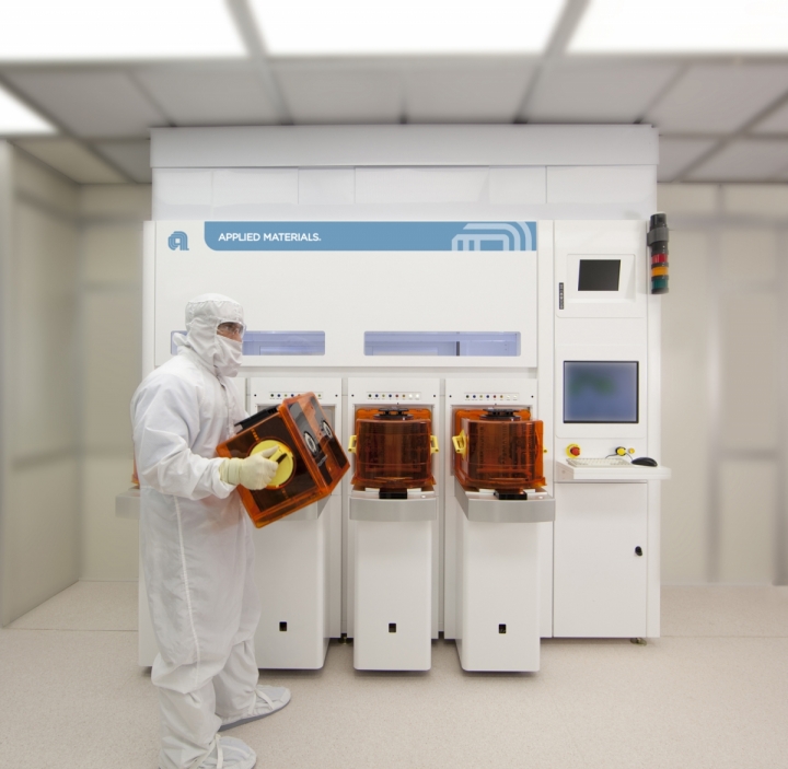
Applied Materials, Inc. (AMAT) has unveiled a new Applied Varian VIISta Trident system.
The semiconductor processing tool manufacturer claims its new model is the semiconductor industry's most advanced single-wafer, high-current ion implantation system.
Suited to engineering the electrical characteristics of the silicon chip by embedding "dopant" atoms, AMAT boasts the new tool is the only ion implanter proven to achieve the yields necessary for manufacturing high-performance, power-efficient logic chips at the 20nm node.
On this level, optimising dopant activation and suppressing defects in the extension, source/drain junction and contact regions become significant challenges that impede the scaling of high performance transistors.
AMAT reckons its VIISta Trident system is unique as it can be used to precisely tailor dopant concentration and depth profile. Having this control is vital to optimising performance, controlling leakage current and reducing variability in advanced devices.
"A typical advanced logic chip requires as many as 60 implant steps, including co-implant and precision materials modification applications - many of which are critical to device performance. The precision of our VIISta Trident technology is vital to helping our customers achieve profitable yields on their leading-edge designs," notes Bob Halliday, vice president and general manager of Applied's Varian business unit.
"This benchmark performance strengthens Applied's leadership position in providing our customers with leading-edge transistor fabrication solutions. All major foundries fabricating 20nm chips today are using our VIISta Trident systems as tool of record."
Key to the performance of the Trident system is its proprietary dual-magnet ribbon beam architecture for enhanced low energy performance. The system's Energy Purity Module is claimed to practically eliminate damaging, high-energy species that can "smear" the critical transistor channel and lead to increased current leakage and degraded performance.
Integrated cryogenic technology enables production implants as low as -100°C, providing superior process control for transistor matching. This is particularly vital for making embedded SRAM cells for on-chip cache memory, where the six or eight transistors that make up each cell must be precisely matched to enable reliable switching at the low operating voltages required for mobile computing.


