
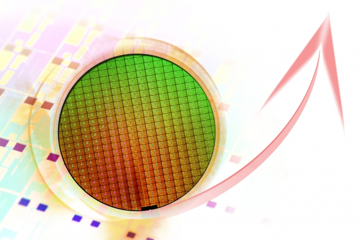
450mm report claims transition will provide 30% cost savings
Future Horizons, a semiconductor consultancy and analyst house, has announced that the European Commission has published a report Future Horizons co-authored with the French firm, Decision, titled Benefits and measures to set up 450 mm Semiconductor Prototyping and to keep semiconductor manufacturing in Europe: The role of public authorities and programmes.
The purpose of the study was to identify the activities required to support research and innovation in the field of advanced semiconductor production and the necessary measures needed to attract investments to support advanced research infrastructures, prototyping and early nanoelectronics manufacturing in Europe.
The report places particular emphasis on 450mm manufacturing with topics including:
- An assessment of the role of the European Commission and governments of member states and regions for the establishment of 450mm manufacturing capabilities, including related value chain aspects, and their overall role in retaining semiconductor manufacturing and advanced nanoelectronics technologies within Europe
- An analysis of potential links between newly established 450mm manufacturing with existing semiconductor manufacturing capabilities and the likely impact on them both at the prototyping and high-volume level.
This report, the result of a 14-month study undertaken between January 2011 and February 2012, involved face to face interviews with senior industry executives across the full industry eco-system. These included advance research institutes, equipment and materials firms, IP providers, IDM, fabless and foundry semiconductor manufacturers as well as end users and public authorities. Interviews were undertaken in Europe, Japan, Korea, Taiwan and the USA, and progress regularly reported and discussed at routine industry led steering group and focus group briefings.
At the time of commissioning the study, there was still some scepticism amongst the industry regarding the 450mm transition; by the end of the study the climate has changed with Intel, Samsung and TSMC now committed to roll out 450mm-ready wafer technology in their latest fab plants, joined by Global Foundries and IBM to form the G450 Consortium in Albany.
Malcolm Penn comments, "The 450mm transition is necessary for the industry to keep up with the underlying 10 percent annual growth in wafer fab capacity demand. The wafers are 2.25 bigger in surface area, and therefore the number of ICs produced per wafer, making it more efficient to build a single 450mm fab rather than two 300mm fabs The 450mm transition is also expected to deliver a 30 percent cost reduction thus providing 450mm wafer fabs with a definite competitive advantage over 300mm."
Penn further commented "Even though reluctant and hesitant at first, the equipment and material industry is now asking to be fully associated with the transition to 450mm and there is a tacit acceptance that any technology and process issues related to the 450mm development will be solved in due time. It is also highly unlikely there will be parallel development on 300mm ITRS node development once 450mm is in full production before the end of the decade."
Because of the potential long-term ramifications for the industry, the study deeply probed the underlying opinions towards the industrial, technological and economic aspects of the transition. One of the conclusions drawn in the report is that the 450mm transition will happen and that it will very likely be the final wafer scale up for the industry. It will also define the geographical locations of the next (and perhaps final) ten to fifteen most advanced semiconductor production areas worldwide. With 8nm likely to be the first node only available on 450mm platforms for volume production, meaning, we can then expect that post-CMOS technologies will be exclusively developed on 450mm platforms.
The report can be downloaded at the Commission's website at: http://cordis.europa.eu/fp7/ict/nanoelectronics/documents/450mm-final-report.pdf


