
A new bright SPARK in semiconductor defect inspection
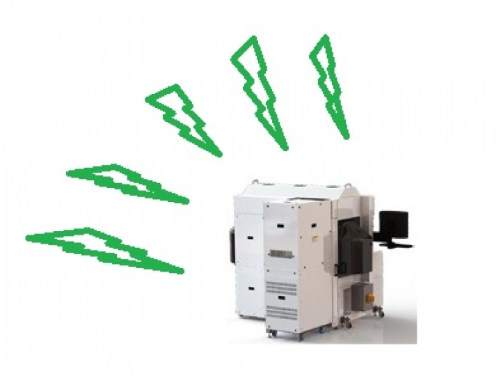
Nanometrics has announced that its SPARK-API macro defect inspection system has been qualified by a leading device manufacturer in Asia for advanced 2X nm devices.
The system is being used in the development of advanced 3D wafer-scale packaging (WSP) processes for next-generation memory and logic devices, which are currently scheduled for high-volume production later this year.
The SPARK-API was qualified at multiple inspection
steps, including bonding quality, wafer thinning and backside processing for
through-silicon via (TSV) applications. "The SPARK was selected for its
versatility to address the wide range of process control inspection needs in
this emerging segment of WSP," commented Lars Markwort, vice president of the
Inspection Business Unit at Nanometrics.
"The SPARK platform ideally meets the high-volume manufacturing needs of 3D-WSP with its high throughput and low cost of ownership enabled by capturing a full wafer image in a single "˜shot.' The SPARK's unique technology detects both large-area and small particle defects, as well as residue from previous process steps and voids in the bond layer from improper bonding."
"We are pleased to have our SPARK-API system selected
by one of our leading customers, along with the opportunity to work with an
industry leader on this rapidly emerging new technology," added Tim Stultz,
president and chief executive officer of Nanometrics.
"This latest selection further advances our strategy to expand our served markets by entering the inspection market as well as to increase our participation in growth segments such as 3D device integration. The SPARK system highly complements the position we have established with our UniFire system for TSV, micro-bump and advanced metallisation process control, providing a comprehensive, end-to-end solution for our customers and their emerging applications in 3D-WSP."
The SPARK can be used for macro defect inspection
across semiconductor manufacturing lines, providing cost-effective and
extendible technology for mask, wafer backside, lithography, and wafer-scale
packaging. It can be used on patterned and unpatterned wafers.
When used alongside, or combined on the Lynx platform with other Nanometrics solutions for critical dimension, overlay and topography, manufacturers can achieve low cost of ownership, high information throughput and a small fab footprint for advanced process control metrology and inspection.
Full wafer surface images are processed in near real-time to extract a broad range of defects. The SPARK system is sensitive to large area defects down to small defects - Nanometrics says beyond the sensitivity of traditional macro inspection systems. The platform supports a wide range of surface materials and topographies and can be used for inspection at nearly every stage of the semiconductor production flow. Also, CD uniformity information can be extracted on production wafers.
The tool has 1-3 µm sensitivity at over 120 wph on patterned wafers and 0.5 µm sensitivity at greater than 120 wph on unpatterned wafers. The tool is also capable of edge inspection and back-side inspection is an option.


