
Ultratech To Use IBM's Semiconductor Bump & Packaging Technology
Ultratec, a supplier of lithography and laser-processing systems used to manufacture semiconductor devices, has acquired the rights to a collection of patents from IBM.
These include fundamental patents in packaging such as
C4 bumping, Ball Grid Arrays, lead-free solders and 3D packaging.
Representing both U.S. and foreign patents, the portfolio includes claims directed at methods of making, at compositions and at structures of semiconductor devices. This acquisition strengthens and broadens Ultratech's offerings to facilitate advanced packaging at the lower device nodes.
"Ultratech has periodically purchased patents that it views are key to our business," noted Ultratech Chairman and CEO Arthur W. Zafiropoulo. "The acquisition of these patents from IBM is the continuation of that strategy to ensure that our customers receive the highest technology content in their products. This acquisition reinforces our commitment to remain at the forefront of providing equipment with leading-edge technology and low cost-of-ownership advantages for our global customer base."
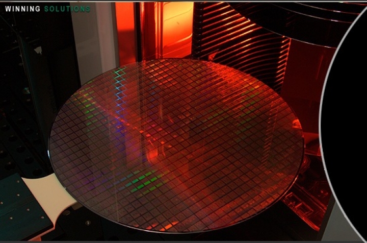
Founded in 1979, Ultratec 's advanced lithography
products are designed for bump packaging of integrated circuits and high-brightness
LEDs (HB-LEDs). The firm also developed laser spike anneal technology, which
increases device yield, improves transistor performance and enables the
progression of Moore's Law for 32-nm and below production of state-of-the-art
consumer electronics.


