
News Article
EVG's Bonding & Debonding Platform For 3D ICs & TSV
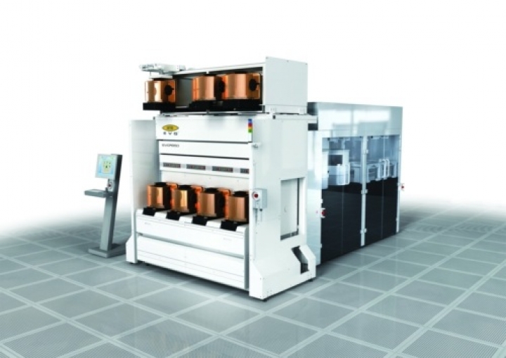
EV Group (EVG), a supplier of wafer bonding and lithography equipment for the MEMS, nanotechnology and semiconductor markets, has revealed the EVG850TB/DB automated temporary bonding and debonding system.
The tool is built on the company's new XT Frame platform, which has been optimised to support thin-wafer processing for high-volume 3D IC and TSV (through silicon via) manufacturing. A combination of hardware and software design enhancements enables double the processing throughput over EVG's previous-generation, industry-benchmark platform to up to 40 stacks per hour.
The XT Frame-configured EVG850TB/DB is designed for EVG's open materials platform approach, which enables the use of a wide range of adhesives from various materials suppliers. This approach provides customers with a flexible choice of bonding materials supporting ZoneBOND and other technologies.
"Temporary bonding and debonding of device wafers to wafer carriers for thin-wafer processing are critical steps to enabling the successful integration and implementation of 3D ICs into high-volume production," pointed out Thorsten Matthias, Business Development Director, EV Group.
"To this end, advances in wafer bonding are necessary to support the efforts of early 3D IC/TSV adopters as they move ever-closer to attaining this goal. Our new XT Frame-configured EVG850TB/DB builds upon our core expertise to provide production-ready solutions for our customers to facilitate their rapid ramp from development and integration to high-volume manufacturing. It is designed from the ground up to enable the highest productivity and yields in thin-wafer processing."
Built on the company's new XT Frame platform, the EVG850TB/DB is capable of accommodating up to nine process modules, doubling the previous maximum processing capability of EVG's temporary bonding and debonding systems. The new XT Frame design enables highly efficient continuous mode operation (zero idle time) capability via an ultra-fast handling system, up to four FOUP (front opening unified pod) load ports, and a material buffer in the form of a local FOUP storage system that holds up to 10 additional FOUPs.
The platform also features an in-line metrology module option to enable real-time monitoring of the bonding/debonding process, enabling high yields and helping to lower production costs for thin-wafer processing. In addition, the EVG850TB/DB has been qualified for all bonding and debonding methods, including low temperature debonding methods like ZoneBOND technology with EZR (Edge Zone Release) and EZD (Edge Zone Debond) modules.
The EVG850TB/DB built on the new XT Frame platform is now available for shipping.


