
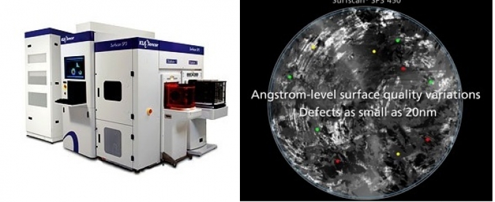
Unpatterned 450mm Wafer Defect Inspection Tool From KLA
KLA-Tencor Corporation has announced the installation of its first process control systems capable of handling and inspecting 450mm wafers.
The new configuration of the Surfscan SP3 platform is called
the Surfscan SP3 450.
Fully automated, these unpatterned wafer inspection systems are designed to meet the demanding defect and surface quality characterisation requirements of the 20nm node and beyond, enabling control of the manufacturing process for 450mm polished silicon and epitaxial silicon substrates. The Surfscan SP3 450 also delivers critical capability for manufacturers of 450mm process equipment, such as wet clean tools, CMP pads, slurries and polishers, film deposition tools and annealing systems.
"Optimisation of wafer quality and cleaning
performance are important first steps toward demonstrating the potential
economic benefits of the wafer size migration," said Hans Lebon, fab
manager at imec, a nanoelectronics research centre based in Leuven, Belgium.
"Wafer manufacturers need to deliver substrates with pristine surfaces to meet chipmakers' tight specifications. Equipment manufacturers need to ensure that they are not adding defects; that cleaning processes are effective; and that film quality is carefully controlled over a larger wafer area. The new Surfscan SP3 450 inspection system will help imec characterise the defectivity and surface quality of the wafer, map film thickness and roughness uniformity, and even identify annealing issues. We feel that it's a critical enabling tool for the transition to 450mm."
"Whether their wafers are 300mm or 450mm in
diameter, our customers will need the performance that the Surfscan SP3 can
deliver at the 20nm node and beyond," added Ali Salehpour, senior vice
president and general manager of the Surfscan / ADE division at KLA-Tencor.
"The SP3 remains the only unpatterned inspection platform in the industry to use sensitivity-enabling deep ultra-violet (DUV) illumination, and it is the only tool of its kind with the ability to generate high-resolution maps of surface quality. Another advantage of the 450mm version of the Surfscan SP3 is that the performance and reliability of its optics and algorithms have already been proven on the more than fifty 300mm SP3's installed at advanced development and production sites around the world. Confidence in their inspection platform will allow our customers to focus their engineering efforts on advanced technology development."
Multiple orders have been received for Surfscan SP3
450 systems, from a range of leading-edge integrated circuit, substrate and
process equipment manufacturers and a nanoelectronics research centre. Several
of these systems have already been shipped.
The Surfscan SP3 is also available in a 300mm-only version and a 300mm/450mm bridge configuration. SP3 models are designed to match among themselves and correlate to previous-generation Surfscan SP2 and SP2XP systems, preserving the factory's baseline and offering flexibility for routing work in progress.


