
AMAT Breaks Barriers In Copper Interconnect Technology
Applied Materials (AMAT) reckons it has pushed the boundaries of interconnect technology, the pathways that connect the billions of transistors on a chip.
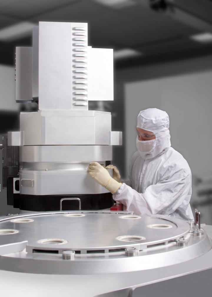
The firm has unveiled the Applied Endura Amber PVD system. Featuring revolutionary copper reflow technology, the Amber system is claimed to be the only single-chamber solution proven to enable void-free copper structures at the 1Xnm node - a critical challenge in the manufacturing of advanced logic and memory devices.
This technology enables the deposition of the vital wiring seed layer and AMAT says it has no foreseeable node limit. Over thirty chambers have already been shipped to leading chipmakers.
"The Applied Endura Amber system delivers a
breakthrough solution for scaling interconnects beyond the 20nm node while
maintaining good production yields," said Sundar Ramamurthy, vice president
and general manager of Applied's Metal Deposition Products business unit.
"Applied has extended its leading PVD technology with a unique system that achieves rapid, void-free fill of these structures at virtually any device node. We're seeing strong customer momentum for the Amber system with more than 30 chambers already in the field. Systems are already qualified as tool of record at leading logic and memory device manufacturers," he continued.
Today's high-density microchips feature complex, multilevel networks with more than 60 miles of copper wiring and as many as 10 billion vertical connections, or vias, between layers. Moving forward, these numbers will significantly increase, with interconnect structures becoming much narrower and deeper, making it extremely difficult for conventional technologies to completely and reliably fill the structure with copper. At the 1Xnm node, this is a major concern, since a single void can render the chip useless.
Applied's Amber copper reflow technology solves this critical challenge by turning the small size of these features from a problem to an advantage. Using capillary action, the deposited copper is drawn into even the smallest features, filling from the bottom upwards to enable rapid, void-free fill from the smallest to the largest features on any die layout.
The Amber system is built on the innovations pioneered with the highly-successful Applied Endura CuBS RFX PVD system. The CuBS RFX system's unique selective PVD technology provides the precise deposition profile - thicker at the bottom and no copper overhang - that is essential for the subsequent reflow process.
The Applied Endura Amber PVD system is one of several new products to be highlighted by AMAT at SEMICON West 2012 from July 10th to 12th.


