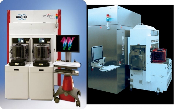
Bruker's Semiconductor Metrology Tools For 450mm Wafers

At SEMICON West 2012, Bruker revealed three new 450mm
X-Ray and AFM semiconductor metrology products to support the industry's
transition to larger wafer production.
These new products include the InSight-450 3DAFM from Bruker's Nano Surfaces division and both the next generation of the D8 FABLINE and the new S8 FABLINE-T X-ray systems from Bruker's AXS division. All three metrology systems are designed to meet the industry roadmap challenges at future technology nodes on the larger 450mm wafer size, enabling both greater product capability and reliability for semi development and production facilities.
Eliminating the need for model setup, and providing
TEM-like accuracy in fractions of the time without wafer damage, Bruker's
automated atomic force microscopes (AFMs) have proven essential tools for
critical technology development and continued process control in production
since 200mm wafer development.
Similarly, Bruker's X-ray metrology has a long tradition of providing a reliable, accurate and non-contact method of characterising various essential semi parameters without the need to use a reference. The wafer size transition from 300mm to 450mm represents another critical technology inflection point that is now supported by Bruker's core metrology technologies.
"Bruker's significant commitment to the SEMI industry is embodied in these three exciting new 450mm-compatible products," stated Bruker AXS division president Frank Burgäzy. "Both X-Ray and high-resolution AFM technologies have been identified by the 2011 International Technology Roadmap as critical for the success of future semiconductor technology nodes, and Bruker is uniquely placed with our technologies to address these future needs. We are very pleased to be part of this critical wafer size transition, and feel that these systems are another indication of our continuing determination to enable the steady advance of semiconductor technology with production-worthy X-ray and AFM metrology solutions."
InSight-450 3DAFM
Based on the InSight 3DAFM platform for 300mm, the
InSight-450 3DAFM is ideally suited for a broad range of roughness, depth and
CD applications. Capabilities include bare wafer process validation, roughness
characterisation and pit/bump/scratch defect metrology; incoming substrate
qualification; thin film and epitaxial deposition performance with micro/nano
roughness and angstrom-level step height precision; etch depth metrology for
process development and control, in-line resist profile measurements of CD,
SWA, and LER with full TEM-like profiles; and CMP flatness performance to
monitor dishing and erosion.
The flexibility of the InSight 450mm AFM means all of these applications are available in a single tool, thus reducing overall cost for metrology. The InSight-450 3DAFM provides this capability with no modeling required, full NIST traceability and no material or wafer damage, making it the ideal tool to provide early learning in 450mm process development with scalability to 450mm production.
FABLINE X-ray Systems
Bruker's next-generation D8 FABLINE is equipped with
the latest high-brilliance X-ray sources, detector technology and user-friendly
software for improved data analysis. The system provides a broad range of
in-line, thin film X-ray measurements for FEOL and BEOL process monitoring on
blanket or product wafers. It is ideally suited for determining thickness,
composition and strain in SiGe, SiC, SOI, III-V-on -Silicon, as well as
composition and thickness for metal films and stacks, including ALD layers.
Bruker has also developed the new S8 FABLINE-T TXRF
(Total X-ray Reflection Fluorescence) for non-destructive trace metal and light
element contamination analysis in order to continue the penetration into the
semiconductor market. New and emerging device processing creates metal
contamination control challenges for IC manufacturing and the latest
state-of-the-art of X-ray instrumentation will be required to face these
challenges.


