
Intel Invests $4.1 billion In ASML 450mm & EUV Lithography
Intel Corporation has entered into a series of agreements with ASML aimed at accelerating the development of 450mm wafer technology and extreme ultra-violet (EUV) lithography totalling EUR3.3 billion (€3.3 billion or approximately $4.1 billion).
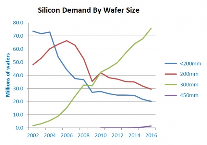
Continued research and development in the field of lithography is critical to the long-term growth of the semiconductor industry.
Intel has invested an extra €829 million (approximately $1.0 billion) to shorten the schedule for deploying the 450mm wafers and extreme ultra-violet (EUV) lithography equipment by as much as two years. This is aimed to at making significant cost savings and other productivity improvements for semiconductor manufacturers.
The multi-party development program includes a cash contribution by Intel to fund relevant ASML R&D efforts as well as equity investments in ASML. The first phase of this program consists of Intel committing to R&D funding of €553 million (approximately $680 million) to assist ASML in accelerating the development and delivery of 450mm manufacturing tools, as well as an equity investment of €1.7 billion (approximately $2.1 billion) for approximately 10 percent of ASML's pre-transaction issued shares. Intel will record the R&D investment as a combination of R&D expense and pre-payments on future tool deliveries.
The second phase of the program depends upon ASML shareholder approval. It includes an additional commitment by Intel of R&D funding of €276 million (approximately $340 million) in ASML, focused on accelerating EUV, as well as an equity investment of €838 million (approximately $1.0 billion) for an additional 5 percent of ASML post-transaction issued shares.
Intel will then hold a total of 15 percent of ASML's issued shares. The total equity investment will be €2.5 billion (approximately $3.1 billion). As part of these agreements, Intel is also committing to advanced purchase orders for 450mm and EUV development and production tools from ASML.
Both phases of the program are subject to standard closing conditions, including customary regulatory approvals. The companies expect both phases of the transaction to close after the shareholder vote in the third quarter.
"Productivity improvements driven by enhanced wafer manufacturing technologies, especially larger silicon wafers and enhanced lithography technologies with EUV are direct enablers of Moore's Law, which delivers significant economic benefits to consumers," said Brian Krzanich, Intel senior vice president and chief operating officer.
"The transition from one wafer size to the next has historically delivered a 30 to 40 percent reduction in die cost and we expect the shift from today's standard 300mm wafers to larger 450mm wafers to offer similar benefits. The faster we do this, the sooner we can gain the benefit of productivity improvements, which creates tremendous value for customers and shareholders."
ASML intends to sell up to a 25 percent aggregate stake in the company (on a post-transaction basis) to Intel and other semiconductor manufacturers in this program. ASML is currently in discussions with other customers and has publicly indicated it expects others in the industry to participate in the R&D and equity program. Regardless of the outcome of ASML's discussions with other customers and upon completion of this two-phase program, Intel's ownership stake in ASML will not exceed 15 percent of ASML's post-transaction issued shares and will be subject to lock-up and voting restrictions.
Intel intends to fund its R&D and equity investments in ASML from cash on hand at its offshore subsidiaries.
"We are extremely encouraged that Intel has made these investments, which will benefit every semiconductor manufacturer in the industry," said Eric Meurice, president and chief executive officer of ASML. "We hope to be able to announce additional investments by our other customers in the coming weeks."
A critically important aspect of this transaction is
the additional funding it provides for ASML's EUV development
program. When deployed in conjunction with 450mm wafer production, the
productivity and cost benefits of EUV will be substantial for Intel and other
semiconductor manufacturers. Intel was involved in the formation of the first
EUV consortium in 1997. With these additional R&D investments for EUV, ASML
and Intel hope to help lead the semiconductor industry in the transition to
this critical technology.


