
imec 300mm DSA Development Extends EUV Lithography
Imec and Tokyo Electron (TEL) aim to accelerate their Directed Self-Assembly (DSA) activities at imec's latest 300mm fab-compatible DSA process line.
DSA is gaining momentum in extending optical lithography beyond its current limits. As an alternative patterning technology, DSA enables frequency multiplication through the use of block copolymers. When used in conjunction with an appropriate pre-pattern that directs the orientation for patterning, DSA can reduce the pitch of the final printed structure.
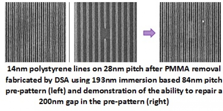
What's more, DSA can be used to repair defects and repair uniformity in the original print. This repair feature is especially useful in combination with EUV lithography, which today is characterised by local variation in the critical dimension, especially in case of small contacts.
Imec previously announced the successful implementation of the world first 300mm fab-compatible DSA process line all-under-one-roof in imec's 300mm cleanroom fab in February 2012.
In the last two years, both companies have been actively engaged in DSA development. Based on promising results achieved on imec's 300mm DSA process line, the two organisations will now expand their focus to explore DSA as a cost-effective and manufacturing viable patterning technique for 2x and beyond technologies.
Recent evaluations have shown the feasibility of DSA to enable frequency multiplication through the use of block copolymers. Line features as small as 12.5nm and 25nm contact holes have been patterned on 300mm substrates at imec using pre-patterned lithography followed by DSA.
In recent experiments using pre-patterned EUV holes, on wafers processed on TEL's CLEAN TRACK™ LITHIUS Pro coater/developer interfaced to ASML's NXE:3100, DSA repaired defective features, lowered line edge roughness (LER) and improved critical dimension (CD) uniformity.
However, for widespread DSA use, lower defect levels are required, and DSA needs to be integrated into existing process flows.
Imec and TEL are therefore investigating various integration scenarios for line and hole patterning. Furthermore, comprehensive evaluations to understand material and process interactions on CD uniformity, LER and defect levels are planned. Imec and TEL aim at delivering electrical functional devices using DSA.
To push the capabilities of DSA beyond lab-scale environments, one of the world first 300 mm fab-compatible DSA process lines all-under-one-roof was recently implemented in imec's 300 mm clean room fab.
In addition to TEL's especially configured DSA coater/developer managing gallon-sized quantities of block copolymers, and TEL's dedicated etch system supporting the DSA pattern transfer, imec has the necessary metrology, cleaning and pattern transfer toolsets. To complete the DSA process line and accelerate R&D on DSA at imec, TEL will provide imec with new hardware within the next few months.
"With specially configured DSA coater/developer and etch systems at imec, we have the capability to explore DSA as a potential candidate for next-generation patterning technology", commented Chung Gishi, Executive VP of Tokyo Electron Ltd. "We hope to understand the critical processes necessary to move early stage development into volume production to benefit our customers".
"DSA continues to show much promise as part of the toolbox for advanced sub-20 nm patterning. Our collaboration with Tokyo Electron has enabled us to rapidly implement DSA processing knowledge that has been developed in academia at the group of Prof. Paul Nealey (University of Wisconsin at Madison) into a representative manufacturing environment. We are excited to extend this effort to dedicated newly developed DSA modules. Early access to this equipment allows us to identify and overcome the critical issues to make DSA ready for implementation into the manufacturing processes of our partners." added Kurt Ronse, Director Lithography Department at imec.


