
3D TSV chip market escalating rapidly
Last year, the market value of all the devices using TSV packaged in 3D in the 3DIC or 3D-WLCSP platforms (CMOS image sensors, Ambient light sensors, Power Amplifiers, RF and inertial MEMS) was worth a whopping $2.7 billion.
In a recent report, "3DIC & TSV Interconnects 2012 Business Update" by Yole Développement, this booming sector will represent 9% of the total semiconductor value by 2017, hitting almost $40 billion. 3DIC which typically uses TSV "˜via middle' for memory and logic IC stacking is expected to grow the fastest in wafers as well as in overall value, whereas 3D WLCSP will continue growing at a 18% CAGR.

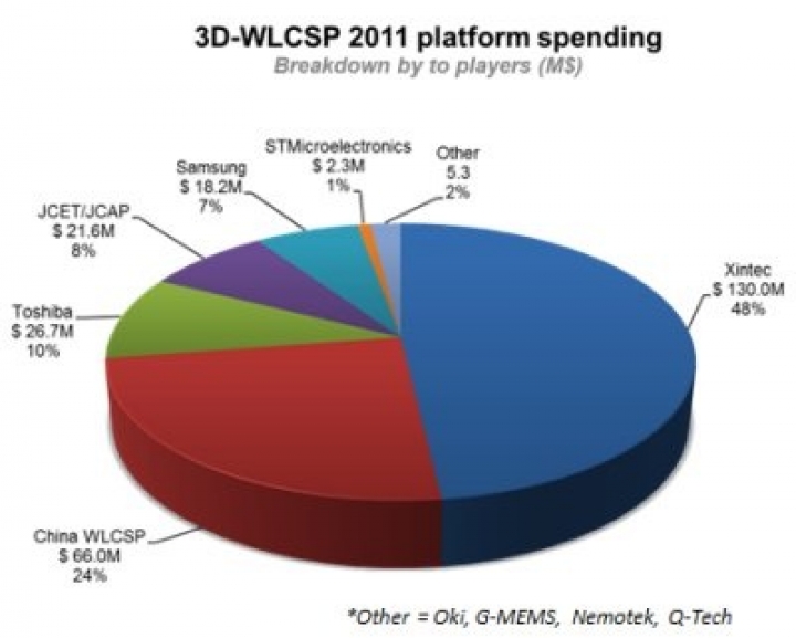
3D WLCSP is the preferred solution today for the efficient assembly of small-size optoelectronic chip like CMOS image sensors. It is also the most mature 3D TSV platform at the moment and Yole predicts the market to hit as much as nearly~ $270 million in 2011 for the "middle-end" processing factories serving this specific market.
More than 90% of the revenues in this area come from low-end and low resolution CMOS image sensors manufacturing (typically CIF, VGA, 1MPx and 2MPx sensors). Xintec in Taiwan is the leader for 3D WLCSP packaging today, followed by China WLCSP, Toshiba and JCAP.
Most of the players provide 3D WLCSP services based on a 200mm wafer-level-packaging industrial infrastructure. Important investments are still expected from major companies to move to 300mm. Indeed, this move to 12" will be necessary to move to the high-end CMOS image sensors market (> 8MPx resolution) were sensors are today on the transition to move from backside illumination to real 3DIC packaging architecture that we will soon call « 3D BSI », where photodiodes will be vertically stacked directly onto the DSP / ROIC wafer and connected by the mean of TSVs.
3DIC technology is foreseen today as a new paradigm for the future of the semiconductor industry as it will enable several more decades of chip evolution at ever lower cost, higher performance and smaller size features.
3D stacked DRAM and 3D Logic SOC applications are expected to be the biggest drivers for the volume adoption of 3DIC technology in the next 5 years to come, followed by CMOS image sensors, power devices and MEMS. The market is currently driven by high-end applications using 2.5D partitioning interposers. Large die FPGAs and ASICs are on the way to be commercialized for industrial applications but are also expected to grow in the near-future in the gaming and smart TV markets.
2013 will probably be the key turning point for the
first true implementation of 3DIC technology in significant volume, driven by
the commercialisation of the hybrid memory cubes of Micron, Samsung, SK-Hynix
and IBM in server and HPC markets.

However, we may need to wait until 2014-2015 before seeing any significant volume adoption of the "˜wide IO interface' concept with TSV in a 28nm application processor chip for mobile / tablet applications. Indeed, given the complexity of the supply chain settlement to successfully deliver real products to the market in such high volumes and complex technology node, it is expected that some level of industry consolidation is needed to gather the front-end, middle-end to back-end assembly & test operations under the umbrella of one unique, single player entity.
Wafer foundry giants Samsung and TSMC are clearly catching-up with this vertical integration trend to meet with the demand from leading fabless companies such as Qualcomm, Broadcom, Marvell, nVidia and Apple, but also with fab-light IC companies TI, STMicro and NEC / Renesas.
Although the middle-end processing space such as bumping services is today almost a "zero margin" business, it is becoming a strategic area to step in, especially when moving to complex chip packaging applications such as 3DIC modules. Recent interest of both wafer foundries and OSAT to invest into this space is quite clear: getting closer to the "˜virtual IDM' business model. If wafer foundries will always make the biggest part of their profits in the front-end wafer processing area, manufacturing of 3DIC modules will need a much stronger integration with middle-end to back-end assembly and test operations, either by expansion or by collaboration through partnership with key packaging subcontractors.
The outlook is looking bright for the future "˜virtual IDM' models that will expand into the 3DIC chip business: we estimate that the global 3D TSV semiconductors packaging, assembly and test market will reach the $8B business value by 2017. About $3.8B of this business will be related to the middle-end wafer processing activity such as TSV etching filling, wiring, bumping, wafer testing and wafer-level assembly. Meanwhile, the back-end operations related to the assembly and test of such complex 3DIC modules will reach an impressive market value of $4.6 billion, representing a clear opportunity for sustainable grow in this "2.0" advanced packaging industry.


