
Graphene potential closer
Researchers devise scalable method for fabricating high-quality graphene transistors
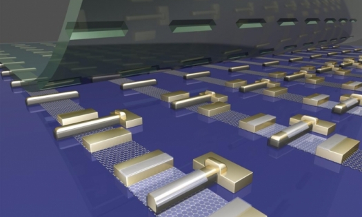
Researchers have developed a method of manufacturing transistors with grapheme that could lead to a consistent and viable manufacturing process for a material that has been showing promise for many years. Graphene, a one-atom-thick layer of graphitic carbon, has attracted a great deal of attention for its potential use as a transistor that could make consumer electronic devices faster and smaller. But the material's unique properties, and the shrinking scale of electronics, also make graphene difficult to fabricate on a large scale. The production of high-performance graphene using conventional fabrication techniques often leads to damage to the graphene lattice's shape and performance, resulting in problems that include parasitic capacitance and serial resistance.
Now, researchers from the California NanoSystems Institute at UCLA, the UCLA Department of Chemistry and Biochemistry, and the department of materials science and engineering at the UCLA Henry Samueli School of Engineering and Applied Science have developed a successful, scalable method for fabricating self-aligned graphene transistors with transferred gate stacks.
By performing the conventional lithography, deposition and etching steps on a sacrificial substrate before integrating with large-area graphene through a physical transferring process, the new approach addresses and overcomes the challenges of conventional fabrication. With a damage-free transfer process and a self-aligned device structure, this method has enabled self-aligned graphene transistors with the highest cutoff frequency to date "” greater than 400 GHz.
The research demonstrates a unique, scalable pathway to high-speed, self-aligned graphene transistors and holds significant promise for the future application of graphene-based devices in ultra"“high-frequency circuits. Authors of the research include UCLA chemistry postdoctoral scholars Lei Liao and Hailong Zhou; UCLA chemistry graduate students Lixin Liu and Shan Jiang; UCLA materials science and engineering graduate students Rui Cheng, Yu Chen, YungChen Lin and Jinwei Bai (now a research scientist at IBM); UCLA associate professor of materials science and engineering Yu Huang; and UCLA associate professor of chemistry and biochemistry Xiangfeng Duan.
Professors Huang and Duan are also members of the California NanoSystems Institute at UCLA. The research was supported by the National Science Foundation, the National Institutes of Health and the U.S. Office of Naval Research. The research was published in the July 2 issue of Proceedings of the National Academy of Sciences.


