
ASML announce results
Only a week has passed since ASML announced the investments of 450mm by manufacturers signalling a change in industry dynamics and the company has confirmed its global strength with another positive quarter results. The company has confirmed confirms steady sales for the remainder of the year and is on track for 2012 second half sales between EUR 2.2 and 2.4 billion.
"We executed H1 2012 as planned and expect sales to remain steady in the second half," said Eric Meurice, President and Chief Executive Officer of ASML. "The second half revenue level is expected to be between EUR 2.2 billion and 2.4 billion and looks sustained by an increase of NAND memory critical layer systems shipments, stability of DRAM memory systems sales, and slower 28/32 nm Logic in the second half compared with the first half. The exact level of sales achieved in the second half will depend on the strength of NAND pick up, itself fueled by new ultrabook PCs and new smartphone ramps."
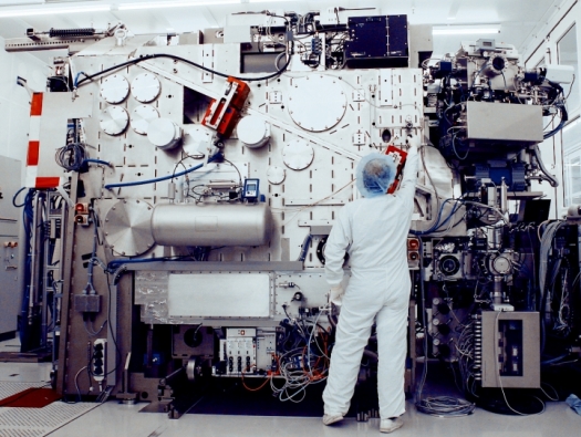
For the third quarter 2012, ASML expects net sales of about EUR 1.2 billion, gross margin of about 43 percent, R&D costs at EUR 145 million and SG&A costs at EUR 60 million. To date they have shipped 30 TWINSCAN NXT:1950i systems which can image 230 wafers per hours. In addition, they have started upgrading TWINSCAN NXT:1950i systems at customer manufacturing sites to this productivity level. Also in this quarter A TWINSCAN NXT:1950i has exceeded the productivity milestone of more than 5,100 wafers in a single day at a customer manufacturing site, 600 wafers more than the previous record achieved three months ago.
"On the technology front, we expect to ship the first of the NXE:3300," Meurice said. "Our production-capable Extreme Ultraviolet (EUV) system, by the end of this year or early next year and the rest of our 11 unit order in 2013. These tools will be used for process development. We are furthermore making progress in preparing EUV lithography for 2014 device production, evidenced by customer commitment to purchase four additional production systems for delivery in 2014. This commitment is enabled by the data gathered on source power increase and by steady performance of the six units already in the field,".
The computational lithography unit Brion delivered enhancements to its leading Mask 3D models and applications, which are required at the 20 nanometer node and below. The full accuracy of the Brion Mask 3D models can now be realized with virtually zero incremental computational cost versus substantially less accurate thin mask models.
The company states that customers have now exposed more than 15,000 wafers on the six NXE:3100 process development systems currently installed. They have now exposed the first wafers on the NXE:3300B EUV scanners. The company has received customer commitment to purchase four additional NXE:3300 systems, raising the total to 15, as customers are accelerating development and preparing for first semiconductor device production on EUV systems in 2014.
With regards to productivity of the EUV source, 50 Watt power capability has been repeatedly demonstrated at a supplier and 105 Watt concept potential has been confirmed in lab experiments, supporting the roadmap to volume production systems starting at 70 wafers per hour. In situ experiments on the NXE:3300 will however still be necessary for full confirmation. The company has completed the expansion of the EUV cleanroom.
On July 9, ASML announced a co-investment program in which customers will potentially contribute up to EUR 1.38 billion over the next 5 years to accelerate the development of 450mm wafer platform and the next generation of EUV systems, expected to enter volume production in the second half of this decade.


