
Researchers develop self-assembling chips
New technique allows production of complex microchip structures in one self-assembling step
Massachusetts Institute of Technology researchers have developed a method to create the complex array of wires and connections on microchips, using a system of self-assembling polymers.
The team hopes the work will pave the way to making more densely packed components on memory chips and other devices.
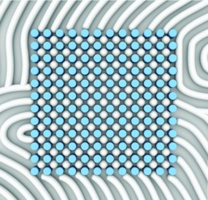
As researcher Caroline Ross, Professor of Materials Science and Engineering at MIT explains, when molecules self-assemble, they have a natural tendency to create hexagonal shapes, as in a honeycomb.
"But this isn't what circuit designers want," she says. "They want [squares and rectangles] with 90-degree angles, so overcoming this natural tendency is essential to producing a useful self-assembling system."
To do this, the team developed a graphoepitaxy technique to create a square-symmetry array of tiny posts on a substrate. The resulting template was used to guide the patterning of the self-assembling polymer molecules.
The researchers found that in addition to producing perfect square and rectangular patterns of tiny polymer wires, the template could also be used to create of a variety of shapes of the material itself, including cylinders, spheres, ellipsoids and double cylinders.
"These complex shapes are possible because the template is coated to repel one of the polymer components, causing a lot of local strain on the pattern," explains fellow researcher, Karl Berggren, from electrical engineering at MIT. "The polymer molecules then twist and turn to avoid this strain, and in so doing rearrange on the surface. So we can defeat the polymer's natural inclinations, and make it create much more interesting patterns."
The researchers also used their system to produce features, such as arrays of holes in the material, with spacings much closer than those achieved using conventional chip-making methods
As they highlight, this means the technique can produce much more closely packed features on the chip than today's methods, a crucial step to packing more components onto a single microchip.
As fellow researcher and MIT visiting student Amir Tavakkoli says: "Fabricating a large area of complex circuitry on a chip using electron-beam lithography could take several months. In contrast, using the self-assembling polymer method would take only a few days."
The researchers admit this is still far too long for commercial manufacturing, but as they explain, this step needs to be done only once to create a master pattern, which can then be used to stamp a coating on other chips in a very rapid fabrication process.
Craig Hawker, a professor of chemistry and biochemistry at the University of California at Santa Barbara who was not involved in this work, added: "There is a growing need and requirement for industry to find an alternative to traditional photolithography for the fabrication of cutting-edge microelectronic devices."
"This work represents a pivotal achievement in this area and clearly demonstrates that structures once considered impossible to achieve by a self-assembly strategy can now be prepared with a high degree of fidelity," he adds.


