
FEI electron microscope targets semiconductor production
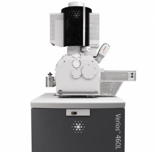
The Verios scanning electron microscope promises sub-nm resolutions on beam-sensitive materials
US-based imaging and analysis systems provider, FEI, has launched a high-resolution scanning electron microscope, the Verios XHR SEM, for advanced semiconductor manufacturing and other materials science applications.
According to FEI, the Verios provides the sub-nanometre resolution and enhanced contrast needed for precise measurements on beam-sensitive materials.
"The Verios XHR SEM extends the lifetime of SEM as an important measurement tool in semiconductor process control labs by allowing engineers to measure beam-sensitive materials and structures that are too small for conventional SEM," says Rudy Kellner, vice president and general manager, Electronics Business, FEI. "When combined with our IC3D software, the Verios is a robust instrument that can provide the precise measurements they need to control processes at the 22nm technology node and below."
Trisha Rice, FEI's vice president and general manager of Materials Science Business adds: "For materials scientists, the Verios will also enable important new insights by extending sub-nanometer imaging and characterization to novel materials being developed today. This will allow researchers to capture the high resolution, high contrast images required, without the need to transition to TEM or other imaging techniques."
The Verios is the second generation of FEI's XHR SEM family. At low kV, where the performance of conventional SEM degrades significantly, the Verios system's advanced optics deliver impressive sensitivity to surface detail.
According to FEI, it allows any user to switch quickly between various operating conditions, maintain sample cleanliness, and obtain sub-nanometre resolution at any accelerating voltage from 1kV to 30kV.
The Verios also introduces optimised signal collection and advanced filtering abilities not only to provide higher and more flexible contrast generation, but also allow for a greater range of samples to be investigated. Many beam-sensitive or non-conductive materials can now be accurately observed at the nanoscale, without any preparation, says FEI.


