
Carl Zeiss leads EUV lithography project
Germany-based collaboration promises to take extreme ultraviolet lithography "to the next level".
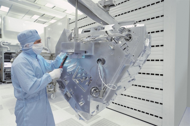
.jpg) Germany-based optics supplier, Carl Zeiss, is collaborating with Germany-based organisations on extreme ultraviolet lithography.
Carl Zeiss, Germany, has joined forces with six other German companies and research institutes to form a joint project, ETIK or “EUV projection optics for 14 nm resolution”, which aims to drive extreme ultraviolet (EUV) lithography forward.
The team aims to boost EUV lithography resolutions to at least 14nm, and intend to have a first technology platform ready by the end of the year that will enable the manufacture of structures as small as 20nm.
The German Ministry of Education and Research (BMBF) has awarded Euros 7 million to the project.
To improve the resolutions, consortium partners are currently researching new manufacturing technologies for the key modules of EUV systems; the illumination system and the projection optics.
For example, a highly flexible optical switching unit has been designed to enhance system performance while researchers have also developed a novel design for the surfaces of the reflection mirrors in the projection lens.
Additional research in optical measuring technology, precision engineering and micro-cooling technology is also planned.
Andreas Dorsel, management board member at Carl Zeiss, says: “We see EUV technology as the key to the microelectronics of tomorrow. The project unites proven experts who will now take EUV to the next level.”
“As a result, we are not only strengthening Germany's leading position in the field of complex optics for lithography systems, but also enabling even more people around the world to acquire state-of-the-art electronic devices by lowering the price of microchips through our research work," he adds.
For this joint project, Bestec, Berlin, is developing machine concepts for a new generation of reflectometers to measure the EUV reflectivity of large mirror surfaces while the Institute for Technical Optics, University of Stuttgart, is testing the concept of flexible setting measuring technology for mirrors with a new type of surface geometry.
IMS CHIPS, Stuttgart, is to provide optical components to ensure the quality of the projection lens. At the same time, the Fraunhofer Institutes for Electron Beam and Plasma Technology, Dresden, Applied Optics and Precision Engineering, Jena and Material and Beam Technology, Dresden, are providing scientific-technical services to improve the surface quality of reflective optical components.
Germany-based optics supplier, Carl Zeiss, is collaborating with Germany-based organisations on extreme ultraviolet lithography.
Carl Zeiss, Germany, has joined forces with six other German companies and research institutes to form a joint project, ETIK or “EUV projection optics for 14 nm resolution”, which aims to drive extreme ultraviolet (EUV) lithography forward.
The team aims to boost EUV lithography resolutions to at least 14nm, and intend to have a first technology platform ready by the end of the year that will enable the manufacture of structures as small as 20nm.
The German Ministry of Education and Research (BMBF) has awarded Euros 7 million to the project.
To improve the resolutions, consortium partners are currently researching new manufacturing technologies for the key modules of EUV systems; the illumination system and the projection optics.
For example, a highly flexible optical switching unit has been designed to enhance system performance while researchers have also developed a novel design for the surfaces of the reflection mirrors in the projection lens.
Additional research in optical measuring technology, precision engineering and micro-cooling technology is also planned.
Andreas Dorsel, management board member at Carl Zeiss, says: “We see EUV technology as the key to the microelectronics of tomorrow. The project unites proven experts who will now take EUV to the next level.”
“As a result, we are not only strengthening Germany's leading position in the field of complex optics for lithography systems, but also enabling even more people around the world to acquire state-of-the-art electronic devices by lowering the price of microchips through our research work," he adds.
For this joint project, Bestec, Berlin, is developing machine concepts for a new generation of reflectometers to measure the EUV reflectivity of large mirror surfaces while the Institute for Technical Optics, University of Stuttgart, is testing the concept of flexible setting measuring technology for mirrors with a new type of surface geometry.
IMS CHIPS, Stuttgart, is to provide optical components to ensure the quality of the projection lens. At the same time, the Fraunhofer Institutes for Electron Beam and Plasma Technology, Dresden, Applied Optics and Precision Engineering, Jena and Material and Beam Technology, Dresden, are providing scientific-technical services to improve the surface quality of reflective optical components.


