
Heidelberg Reveals Advanced Nano Lithography System
German firm Heidelberg Instruments, a producer of maskless lithography systems, has an order for an advanced DWL 2000 system with sophisticated Gray Scale Exposure capability from Heptagon.
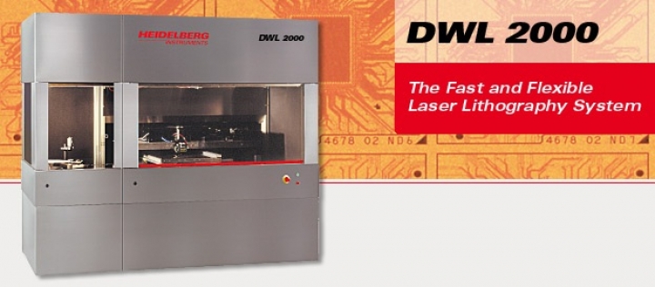
The DWL 2000 laser lithography system is a fast and flexible, high resolution pattern generator for mask making and direct writing. In addition to 2D patterns, the technology of the system can also create complex 3D structures in thick photoresist with a single pass.
With a write area of up to 200 x 200 mm2 the system is the perfect solutionsuited for fast patterning of masks and wafers in MEMS, BioMEMS, Micro Optics, ASICs, Micro Fluidics, Sensors, CGHs, and all other applications that require microstructures.
The system at Heptagon will be used for production of micro optical components for applications in smart phones, mobile devices, gaming consoles, telecoms equipment and supercomputers.
"Gray Scale lithography technology can produce complicated, random, and smoothly or discontinuously contoured material surfaces with a variety of applications in modern optical systems. We implemented Gray Scale lithography in our maskless lithography systems over 12 years ago and through the years have refined this technology in our commercial based systems. This order is a significant step to solidify our position as a global leader in production of direct write systems for applications in Gray Scale Lithography." says Alexander Forozan, Head of Global Sales and Business Development, Heidelberg Instruments
Heptagon is a Singapore-based developer and manufacturer of advanced micro-optics solutions, with an R&D center in Zurich, Switzerland. With nearly two decades of experience in wafer level micro optics, Heptagon produces tiny optical components in large volumes for sophisticated applications in smart phones, mobile devices, gaming consoles, telecoms equipment and supercomputers.
With an installation base in over 40 countries, Heidelberg Instruments is a manufacturer of high precision maskless lithography systems. These systems are used for direct writing and photomask production by some of the most prestigious universities and industry leaders in the areas of MEMS, BioMEMS, Nano Technology, ASICS, TFT, Plasma Displays, Micro Optics, and many other related applications.


