
Global Consortium To Make The Move to 450mm
Innovation and synchronisation among multiple companies do not often go hand in hand. But for the 450mm wafer transition to provide its full benefits, chip makers and their suppliers will need to do more than a simple wafer size scale up.
That may lead the Global 450 Consortium (G450C) to serve as the proving ground for efforts to more closely match the electrical results of production tools.
Addressing this issue, Ron Rinfet, director of Intel's 450 program, has said it will take "a lot of work to align the technical roadmaps, which is one of the roles of the G450C. The suppliers will use this as an opportunity to introduce incredible changes."
Die-to-die matching, scale-up of wafer size along with cost savings are the main technical challenges facing the consortium.
In a presentation during Semicon West, Rinfet showed a slide detailing the role film variability in die to die matching, which will require cooperation on die-level electrical test results, uniform plasma density, improved thermal and thickness control, optimised pumping, and improved film stress management.
The 450 transition program, started at Sematech but now under CNSE's management, has included tool performance specifications for several years, with Sematech program managers conducting day-long seminars on the performance targets of a range of 450mm tools.
Earlier this year, Qualcomm's senior vice president of engineering, Michael Campbell, spoke at the Advanced Semiconductor Manufacturing Conference in Saratoga Springs in New York state. He emphasised Qualcomm's desire to make electrically compatible versions of the same mobile phone processors at two or more fabs.
Currently, Qualcomm needs to use four different libraries for its foundry partners, adding to design complexity. And Campbell said getting two fabs within the same foundry to produce electrically compatible chips is a struggle. He pointed to the synchronisation efforts at G450C as a means of solving the tool and fab matching goals needed by high-volume fabless companies such as Qualcomm.
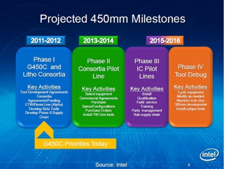
Initially, the consortium's main job is to move tools into the new NFX (NanoFab Xtension) building, nearing completion at the College of Nanoscale Science and Engineering (CNSE) in Albany, New York State. From 2013 onwards, the pilot line will serve as a test bed for methods to more closely align tool outputs, among other goals.
The G450C members currently include Intel, IBM, GLOBALFOUNDRIES, Samsung, and TSMC and CNSE.
Kirk Hasserjian, a vice president at Applied Materials, said there may be only five or six companies processing 450mm wafers, reflecting a savagely Darwinian selection process. During the current 300mm generation, about 25 companies are processing 300mm wafers, down from about 75 at the peak of the 200mm diameter.
In a consolidating industry, companies may rely more heavily on common components in order not to waste R&D dollars. Hasserjian emphasised the need for the chipmakers to move to 450mm at roughly the same time using similar design rules.
The clout of such few equipment buyers puts the G450C members in a strong position to ask for coordinated technical targets as they innovate their patterning, deposition, and other processes. And the equipment companies must deliver a further three nodes on 300mm tools as well, requiring leading edge equipment at both the 300mm and 450mm wafers sizes - an expensive prospect.
Scaling itself will become increasingly thorny as 450mm production begins late in this decade. "DRAM, flash, and logic devices are all hitting fundamental barriers, requiring more atomic-scale deposition," said Akihisa Sekiguchi, a corporate marketing director at Tokyo Electron Ltd. (TEL). Sekiguchi quoted dire forecasts from consultancy IBS predicting that the cost per function is now on an upward curve. "Concurrent development on 300 and 450 tools at the bleeding edge is not sustainable," he argued.
With R&D funds already stretched to the hilt with the demands of device scaling, equipment companies have a favourable view of Intel's roughly $4 billion investment in ASML, which is aimed primarily at readying EUV scanners capable of processing 450mm wafers at high throughputs.
Dean Freeman, manufacturing analyst at Gartner, said he was told that Intel made a private investment in Nikon to prepare the 450mm-capable immersion ArF scanners.
While several executives at major equipment vendors said they would welcome similar investments from Intel to bolster their 450mm development programs, a senior IBM executive said the Intel-ASML relationship may prove to be unique.
ASML holds a virtual monopoly in the EUV tool field, providing the firm with more leverage than any other vendor over when the complete 450mm toolset will become available. Without ASML being fully on board, 450mm at 10nm and below design rules wouldn't go forward. For all the other major tool types, more than one vendor exists, relieving Intel of the need to make direct investments, the IBM executive speculated.
The G450C leadership points to the consortium's investment in a 450mm wafer bank as a means of supporting all the interested tool vendors, according to Michael Liehr, general manager of the G450C. "We are making a large investment in wafers," said Liehr, who earlier worked at IBM before joining CNSE.


