
Sony Unveils World's First Stacked CMOS Image Sensor
Sony Corporation has announced the commercialisation of "Exmor RS," what the firm claims is the world's first CMOS image sensor incorporating a unique, newly-developed "˜stacked structure.'
Shipments will commence in October.
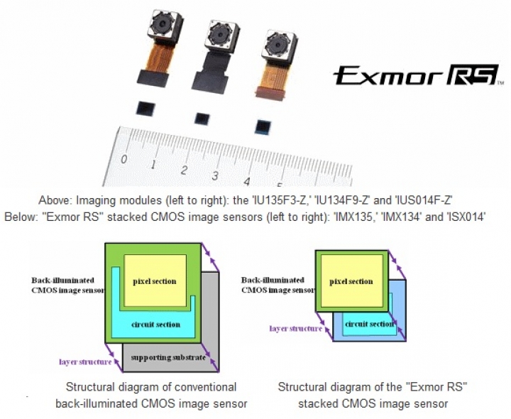
Sony is introducing three models of the "Exmor RS," stacked CMOS image sensor, for use in smartphones and tablets, which it says combine superior image quality and advanced functionality in a compact package. Sony will also launch three corresponding imaging modules incorporating these sensors.
Going forward, the company will continue to evolve its digital imaging products, while aggressively pursuing the further development and expansion of its core "Exmor RS" stacked CMOS image sensor technologies and lineup, in order to deliver increasingly diverse and user-friendly image capturing experiences.
The "Exmor RS" is a CMOS image sensor that adopts a unique "˜stacked structure.' This structure layers the pixel section, containing formations of back-illuminated pixels over the chip affixed with mounted circuits for signal processing, in place of conventional supporting substrates used for back-illuminated CMOS image sensors.
Two of the three "Exmor RS" models Sony is launching are the "˜IMX135', a type 1/3.06 model with 13.13 effective megapixels and the "˜IMX134', a type 1/4 model with 8.08 effective megapixels, which feature "˜RGBW coding' function and "˜HDR (High Dynamic Range) movie' function.
The "˜RGBW coding' function can capture sharp, clear images even when filmed or photographed in low light conditions, such as a dark room or at night by featuring W (white) pixels in addition to conventional RGB (red-green-blue) pixels, and leveraging Sony's proprietary device technology and signal processing to heighten sensitivity without compromising its high resolution.
"˜HDR (High Dynamic Range) movie' function enables two different exposure conditions to be configured within a single screen when shooting, and seamlessly performs appropriate image processing to generate optimal images with a wide dynamic range and brilliant colours, even when pictures are taken against bright light. The other "Exmor RS" model is the "˜ISX014', a type 1/4 model with 8.08 effective megapixels, which has a built-in camera signal processing function.
In addition to the higher image quality and superior functionality, the use of a "˜stacked structure' has helped Sony to achieve a more compact size.
Sony will also bring to market three compact auto-focus imaging modules equipped with lens units and featuring auto-focus mechanisms that incorporate these image sensors: the "˜IU135F3-Z,' "˜IU134F9-Z' and "˜IUS014F-Z'. These three imaging modules adopt a newly-designed lens which has been optimised for the industry's smallest 1.12μm unit pixel size to achieve higher resolution.
The "˜IU135F3-Z' is an auto-focus imaging module incorporating a bright, high-resolution F2.2 lens. The "˜IU134F9-Z' (W:8.5 x D:8.5 x H:4.2mm where the dimensions width (W) and depth (D) exclude flexible printed circuits), is thin and compact. The "˜IUS014F-Z' is an all-in-one imaging module that comprises an image sensor with built-in camera signal processing function and built-in auto-focus and picture adjustment function.
Going forward, Sony plans to continue with the proactive development of its "Exmor RS" stacked CMOS image sensors in order to bring to market imaging modules that achieve higher image quality, advanced functionality and an even more compact size. Sony aims to leverage the characteristics of its "˜stacked structure' design to respond to the demand for larger screens in devices such as smartphones, where the amount of space available for embedding imaging modules is limited, and to continue expanding its product lineup to better accommodate its customers' needs.
Demand is growing rapidly for mobile devices such as smartphones and tablets, and Sony is committed to strengthening its production capacity for stacked CMOS image sensors, which combine the dual strengths of advanced functionality and compact size.
On June 22nd the firm announced that it was making capital investment at Sony Semiconductor Corporation's Nagasaki Technology Centre with the objective of increasing the production capacity for stacked CMOS image sensors.
This will enable Sony to act as a driving force for the industry in the future.


