
MAPPER Secures € 80 Million To Advance e-Beam Lithography
Innovator in maskless e-beam direct-write lithography, MAPPER Lithography, has signed a deal for a financing round of € 80 million.
The round is led by the Russian $10-billion investment fund RUSNANO, whose headquarters are in Moscow. RUSNANO, which focuses on the development of the Russian nanotechnology industry through co-investments in nanotechnology projects, will invest € 40 million.
Another € 40 million will be contributed by current shareholders like ADP Industries, the investment vehicle of Mr. Arthur Del Prado, investment firm Parcom Capital (Parc-IT), Hoving & Partners along with Dutch high-end technology suppliers such as Technolution and DEMCON and innovation credits from AgentschapNL. Also other parties such as a number of Dutch individuals and family investment offices will contribute to the total amount.
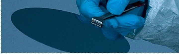
MAPPER Lithography, founded out of Delft University of Technology, is a Delft-based company focusing on the introduction of a groundbreaking maskless lithography infrastructure for the semiconductor industry. Its tools utilise an innovative multiple e(lectron)-beam technology with which next generation semiconductors can be manufactured more cost effectively.
While traditional optical lithography technology requires the use of a costly mask (up to € 2 million per chip module), MAPPER's machines eliminate its necessity. Especially end-users of chips made in relatively low volumes, such as chips for mobile phones and cars, benefit from a maskless solution, since the mask costs are dominating the total costs. The e-beam technology combines high resolution and high productivity "“ up to 100 wafers per hour "“ with a lower cost in production.
The new funds will enable MAPPER to build new Matrix machines with initial throughput of one wafer per hour. The Matrix 1.1 version, which will be built in 2012, uses 1,326 beams to deliver 1 wafer per hour, 10 % of the beams required for the Matrix 10.1 machine, using the final number of 13,260 beams and which is capable of delivering 10 wafers per hour. A clustered version, the Matrix 10.10 will be composed of ten Matrix machines, each machine delivering 10 wafers per hour for total throughput of 100 wph.
In addition, MAPPER will expand its manufacturing infrastructure to 20 machines per year. Next to expanding the existing infrastructure in The Netherlands, part of RUSNANO's investment will be used to establish a manufacturing site in Russia for MAPPER's lens components.
The micro electromechanical (MEMS)-based lens components system, one of MAPPER's major innovations, will ultimately operate with more than 13,260 parallel electron beams simultaneously. The Russian MEMS fab will have sufficient lens element output for 20 machines per year.
The project also aims to develop scientific cooperation with leading Russian research institutes. This investment will open access to cutting-edge technologies that had been closed to Russia before.
MAPPER's cooperation with CEA-Leti, TSMC and others through the IMAGINE program will drive global infrastructure for adoption of maskless lithography.
MAPPER CEO and co-founder Bert Jan Kampherbeek is pleased with the opportunities that arise through the new funds.
He says, "The support that we have received in this round of financing is a strong reflection of our hard work over the past ten years during which we have been developing our groundbreaking direct-write e-beam lithography technology. Today we are close to a promising market introduction within the foreseeable future. I am proud that RUSNANO is supporting our mission with such enthusiasm and substantial investments."
RUSNANO managing director Dmitriy Lisenkov adds, "For RUSNANO, the project with MAPPER Lithography occupies a special place. MAPPER stands at the very beginning of the semiconductor value chain, so this investment strengthens the synergy among RUSNANO's microelectronic projects."
A major achievement with MAPPER's new e-beam direct-write technology at French research institute CEA-Leti's IMAGINE programme has been obtained in resolution: 22-nm dense lines and spaces and 22-nm dense contact holes in positive chemically amplified resist have been successfully resolved. This demonstrated resolution also meets the industry requirement for next generation 14-nm and 10-nm logic technology nodes.
What's more, CEA-Leti and MAPPER announced a three-year continuation of the IMAGINE programme. The extension will involve installation at CEA-Leti of one of MAPPER's first pre-production Matrix systems, offering global players the opportunity to assess maskless lithography technology in a real manufacturing environment.
The industry/research multi-partner programme IMAGINE was initially a three-year project led by CEA-Leti that included leading semiconductor manufacturers TSMC and STMicroelectronics. MAPPER's pre-alpha platform has been installed in CEA-Leti's cleanroom since mid-2009. Because of the outstanding results that have been obtained at CEA-Leti, one of MAPPER's first Matrix systems will be installed at CEA-Leti to enable continuation of the IMAGINE programme for another three years.


