
Ultra Tec Unveils Module For Improved Packaging
A new hardware and software development enhances digital sample preparation system for the decapsulation, thinning and polishing of silicon semiconductor packaged and wafer-level devices
Ultra Tec Manufacturing, has announced the availability of a new End-point Detection Module for the ASAP-1 IPS Selected Area Preparation System.
The End-point Detection Module is a hardware and software enhancement (patent pending) for the ASAP-1 IPS that provides the capability to quantify and act upon the capacitive and/or resistive properties of electronic device and packaging materials, in order to enhance the sample preparation process.
The ASAP-1 IPS is suited for use in silicon and compound semiconductor sample preparation.

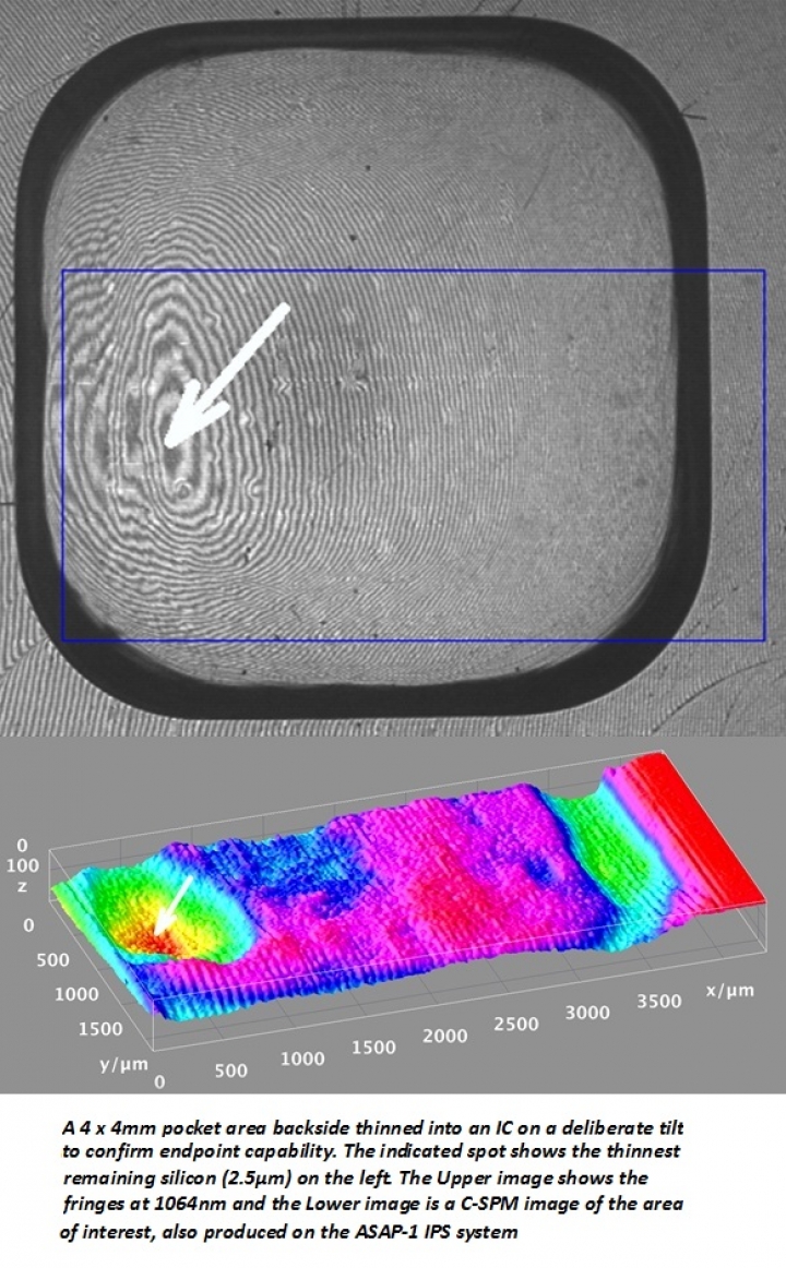
An integrated circuit on a graphics board being prepared on the ASAP-1 IPS in End-point Detection Mode
Controlled microsurgery, with interactive end-pointing, opens the door for improved resolution with SQUID Microscopy, INSB thermography (Lock-In), Thermal Laser Stimulus and similar techniques without fully exposing the die topside or by stopping a few microns before target on silicon from the backside.
ASAP-1 IPS is a digital sample preparation system for the decapsulation, thinning and polishing of packaged and wafer-level devices. Drawing on Ultra Tec's knowledge and market leadership in the selected area preparation area, ASAP-1 IPS has been designed to be specifically "˜device centric' "“ using a combination of advanced programming and tool patterns, force feedback and live machine-vision - to help the user obtain the best results with the highest yield.
The End-point module will be available for demonstration at the upcoming ISTFA 2012 Conference in Phoenix, Arizona.


