
News Article
DCG Wins Multimillion-Dollar Contract For 20nm Process
A major integrated device manufacturer (IDM) has selected DCG Systems' 300mm OptiFIB Viper CE (Circuit Edit) system in a new multi-million dollar contract.
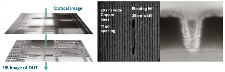
DCG's solution supports 20nm and below processes and is aimed to reduce time-to-market for new technologies.
"No other CE solution offers the same level of performance as the OptiFIB Viper System," said Ketan Shah, General Manager, CE product line for DCG Systems. "DCG ensures the very highest quality and accuracy that is needed to develop the next generation products using the latest process technologies."
"The IDM's selection of the 300mm CE Viper further solidifies our reputation as the proven market leader in semiconductor diagnostic systems," added Dr. Israel Niv, President and CEO of DCG Systems. "DCG Systems is committed to give IDMs the fastest prototyping capability in order to shorten their time-to-market using our cutting edge CE solutions. No other company provides the same combination of live and simultaneous optical and FIB imaging."
Supporting CE needs for 20nm and below process technologies, the 300mm OptiFIB Viper System incorporates DCG's new coaxial photon-ion column, a key feature in this next generation CE product family. The new Viper photon-ion column facilitates beam spot sizes fifty percent smaller than previously possible and enables seamless operation at lower beam energies to avoid device damage during the edit.
Circuit density increases 50 percent at each new major process node, which creates new obstacles in semiconductor diagnostics. Increased density has reduced the size of potential defects down to a few nanometres to create new challenges, such as increased susceptibility to dielectric punch-through by the ions. DCG Systems' high resolution CE solutions are designed specifically to address these new challenges. DCG Systems, Inc., a privately held company headquartered in Fremont, California, supplies semiconductor diagnostic, characterisation and defect localisation solutions.


