
News Article
How To Cut The Cost Of MEMS Device Manufacturing
In the MEMS industry, innovation is key. New MEMS devices will strongly contribute to the double-digit market growth in this industry over the next five years according to Yole Développement.
"InvenSense is one company that can drive the MEMS ecosystem towards more innovation. Indeed, InvenSense is recognised not only as a business leader in MEMS motion sensors, but also as a technology pioneer through its manufacturing platform, which allows for a very high level of integration and development of leading-edge devices," says Laurent Robin, Activity Leader, Inertial MEMS Devices & Technologies at Yole.
"Traditionally, MEMS device designers spend more than fifty percent of their effort designing a fabrication process, inhibiting their ability to quickly prototype, ramp to mass production, or achieve cost-competitive products. InvenSense created the NF-Shuttle program to remove the fabrication barrier and allow MEMS device designers to create their own innovative designs on our established fabrication platform. This approach empowers developers with a direct and rapid path to low-cost, reliable, high-volume manufacturing," explains Martin Lim, Cofounder and Senior Director, Advanced Technology, InvenSense.
InvenSense Inc. is a provider of MotionTracking solutions for consumer electronic devices. The firm's technology can be found in consumer electronic markets including smartphones, tablets, gaming devices, optical image stabilisation, and remote controls for Smart TVs.
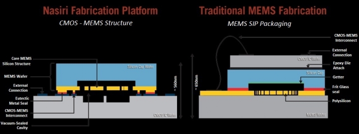
The foundation of Ivensense's MotionTracking devices is the patented Nasiri-Fabrication (NF) process, which combines MEMS on CMOS (also known as CMOS-MEMS) in a small, cost effective standard package. The firgure above shows a schematic of NF versus standard MEMS manufacturing.
Combining a MEMS wafer with an industry standard CMOS wafer allows a reduction in the number of MEMS manufacturing steps and enables wafer-level testing and chip-scale packaging. IvenSense says this in turn cuts back-end costs of packaging and testing and improves overall yield and quality. The company, headquartered in Sunnyvale, California, has also developed low cost, high throughput proprietary test and calibration systems for its motion sensors, which further reduces the back-end costs.
As announced by I-Micronews, powered by Yole Développement, Ivensense has sponsored a webcast, "Developing Your MEMS Products on InvenSense's Nasiri Fabrication (NF) Platform."
This online event will take place on September 19th at 8.00am PDT. In this webcast, MEMS designers will learn how to accelerate product-delivery cycles by leveraging InvenSense's CMOS-MEMS fabrication platform, which is now open to all MEMS developers. The full program is detailed on the website I-Micronews.com in the "Upcoming Webcasts" section.


