
News Article
Novel Fabrication Of Ultra Thin Strong Graphene-based ICs
Integrated circuits, which are in everything from coffeemakers to computers and are patterned from perfectly crystalline silicon, are generally quite thin.
But now Cornell researchers think they can push thin-film boundaries even more - to the single-atom level.
Led by Jiwoong Park, assistant professor of chemistry and chemical biology, the researchers at Cornell succeeded in fabricating single atom-thick sheets of graphene (repeating carbon atoms) and hexagonal boron nitride (BN), an insulator, without the use of a silicon substrate.
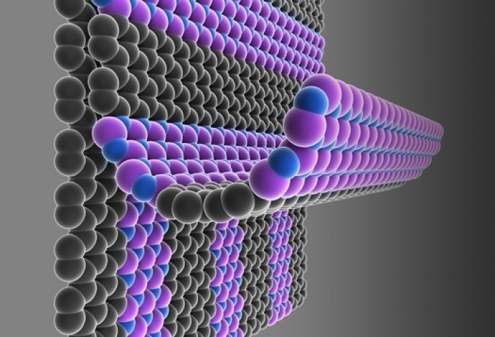
The schematic illustration above shows a single-atom-thick films with patterned regions of conducting graphene (grey) and insulating boron nitride (purple-blue).
The technique used by the scientists, which they call "patterned regrowth", could lead to substrate-free, atomically thin circuits. Although these devices are so thin that they could float on water or through air, they have decent tensile strength and top-notch electrical performance.
"We know how to grow graphene in single atom-thick films, and we know how to grow boron nitride," Park says. "But can we bring them together side and side? And when you bring them together, what happens at their junctions?"
As it turns out, the researchers' patterned regrowth, which employs the same basic photolithography technology used in silicon wafer processing, allows graphene and BN to grow in perfectly flat, structurally smooth films with no creases or bumps. If combined with the final, yet to be realised step of introducing a semiconductor material, this could lead to the first atomically thin integrated circuit.
Devices made using this approach are likely to remain mechanically flexible and optically transparent, allowing transfer to a range of substrates for flexible, transparent electronics. The introduction of two-dimensional semiconducting materials into the sheets would combine the three key building blocks (insulator, metal and semiconductor) of modern integrated circuitry.
Simple really is beautiful, especially in the case of thin films, because photolithography is a well-established technique that forms the basis for making integrated circuits by laying materials, one layer at a time, on flat silicon. Patterned regrowth is a bit like stenciling, Park says.
He and colleagues first grew graphene on copper and used photolithography to expose graphene on selected areas, depending on the desired pattern. They filled that exposed copper surface with BN, the insulator, which grows on copper and "fills the gaps in very nicely." "In the end, it forms a very nice cloth you just peel off," adds Park.
The research team, which includes David A. Muller, professor of applied and engineering physics, is working to determine what material would best work with graphene-boron nitride thin films to make up the final semiconducting layer that could turn the films into actual devices.
The team leveraged its experience in making graphene - still relatively new in the materials world - as well as Muller's expertise in electron microscopy characterisation on the nanoscale. Muller helped the team confirm that the lateral junctions of the two materials were, indeed, smooth and well connected.
Further details of this work are published in the paper, "Graphene and boron nitride lateral heterostructures for atomically thin circuitry," by Levendorf et al, Nature, 488, 627"“632, (30 August 2012). DOI :10.1038/nature11408
This work was supported primarily by the Air Force Office of Scientific Research, and the National Science Foundation through the Cornell Centre for Materials Research.


