
Unlocking The Potential Of Silicon Photonics
Silicon photonics could be a big gun in optics, CMOS, MEMS and 3D technology and create a new breed of photonic devices. But there are a lot of hurdles to overcome...
By blending optical technology with low cost CMOS semiconductor processing, silicon photonics could be the contender with the most potential.
A recent report by Yole Développment entitled, "MEMS : Silicon Photonics : Big Investments, Small Business" has explored the subject in depth.
For starters, the market research firm says that this disruptive technology should enable a new breed of monolithic optoelectronic devices.
The goal of silicon device manufacturers is to deliver economic optical connectivity everywhere, from network level to intra-system level, and eventually to chip-to-chip. Today, except for the light source, all other optical functions, such as modulators, detection, waveguides and intelligence, can be embedded wafer-level at the SOI substrate.
Silicon photonics addresses a number of different kinds of devices. These include individual components and subcomponents which are used as a single function silicon photonics device. Examples include VOA, Mux/Demux, active filters, optical switches or as optical engines combining optics and electronics.
One of the major applications is in transceiver-type products, which include embedded optical modules, transmitters and receivers and active optical cables. Future products could include hybrid packaged devices and 3DICs / integrated optoelectronic chips.
What's more, passive optical elements, such as array wave guides, optical filters, couplers, splitters and polariser arrays, can be created with silicon photonics technologies and integrated with active elements.
Although silicon photonics can address a wide range of applications, very few companies are actually shipping products.
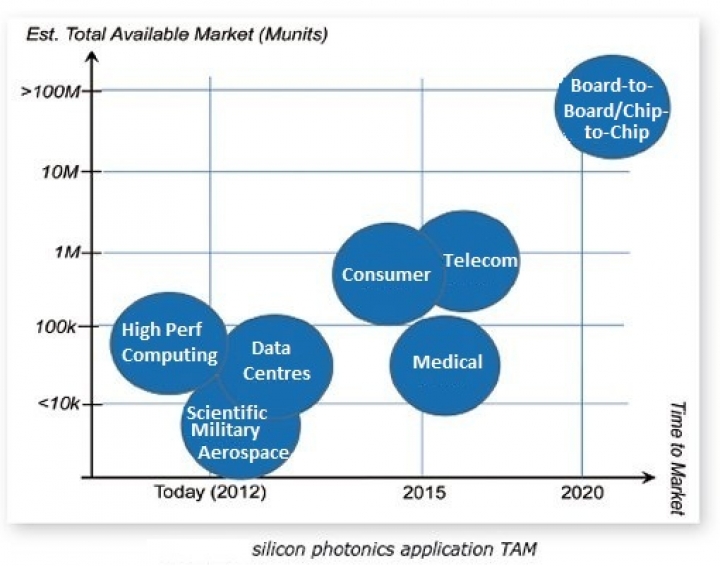
Having said that, there are quite a few potential markets where this technology could have a major impact.
One is in the telecoms sector, specifically in metro and long haul applications. Others are in datacom, where data centres and campus applications are significant, and the consumer area, where connecting desktop PC devices and PCs with HDTVs is something many of us do every day.
Other potential markets for silicon photonics are in HPC & data centres, professional/commercial video, metrology and sensors and in medical and military/aerospace/scientific applications.
But it is in data communications that silicon photonics is expected to dwarf all other applications.
Indeed, major datacom protocols are all moving to high-speed signaling and passing 10Gbps where reach and signal integrity issues are surfacing for both copper and optical technologies. There is a clear trend to surpass 25Gb in datacom protocols and this is where silicon photonics will make sense.
The demand will be driven by a need for low cost, high-speed interconnects supporting ever increasing data rates at and beyond 25Gbps and the desire of reaching distance / data rate not served by vertical cavity surface emitting lasers (VCSELs).
Silicon photonics still faces big industrial and technical challenges, however.
There are currently only a few products using the technology on the market and only several companies have developed integrated product solutions. Also, until significant developments have made, it is likely to be costly and technical mismatch will make silicon photonics even more expensive to implement.
Yole also points out that CAE/CAD programs are almost non-existent and coupled with the need for high volumes and competition with well established VCSEL-based alternatives, advancements in the field could be hindered.

For several years now, silicon photonics projects have been under the umbrella of large-scale R&D projects to set up roadmaps. Today, MPW services foundries are opening and more industrial foundry activities are set up. Generic technologies and generic production platforms are needed to achieve low cost and high volume.
As the future lays in the separation of design and fabrication, this industry is looking for an electronics-like foundry model. The mapping of the players involved in silicon photonics already shows an important number of foundry services.
Although the industry is trying to use as much as possible of existing CMOS processes, 3D ICs technologies will contribute to silicon photonics, especially wafer bonding and 3D interconnects.

Yole says the market is anticipated to triple in five years but business could explode after 2020 as inter and intra-chip communications could make this market grow by a factor of ten. Let's hope it takes off!


