
Veeco IBD System Slashes Defects In EUV Mask Blanks
SEMATECH, a global semiconductor consortium that conducts research and development to advance chip manufacturing, has recently achieved a major breakthrough using Veeco's NEXUS Low Defect Density Ion Beam Deposition (LDD IBD) System to significantly reduce defects from multi-layer deposition of mask blanks used for extreme ultraviolet lithography (EUVL).
Frank Goodwin, Manager of SEMATECH's Mask Blank Defect Reduction program, stated, "EUVL requires a low defect density reflective mask blank, which is considered to be one of the top two critical technology gaps for commercialisation of the technology. Veeco's world-class IBD technology was a major catalyst in helping us to demonstrate low defect levels for the deposition of critical films, and meet the 22 nm defect requirements for EUV mask blanks."
Vivek Vohra, Veeco's Vice President and General Manager, Veeco Ion Beam Equipment, added, "Veeco's NEXUS LDD IBD System has continuously demonstrated the ability to provide low defect density deposition and precise control, which are required to accelerate the development of mask blanks used for extreme ultraviolet EUV, bringing that technology a step closer to high-volume manufacturing. We congratulate the research team at SEMATECH for reaching this milestone and for achieving it on our production-proven system."
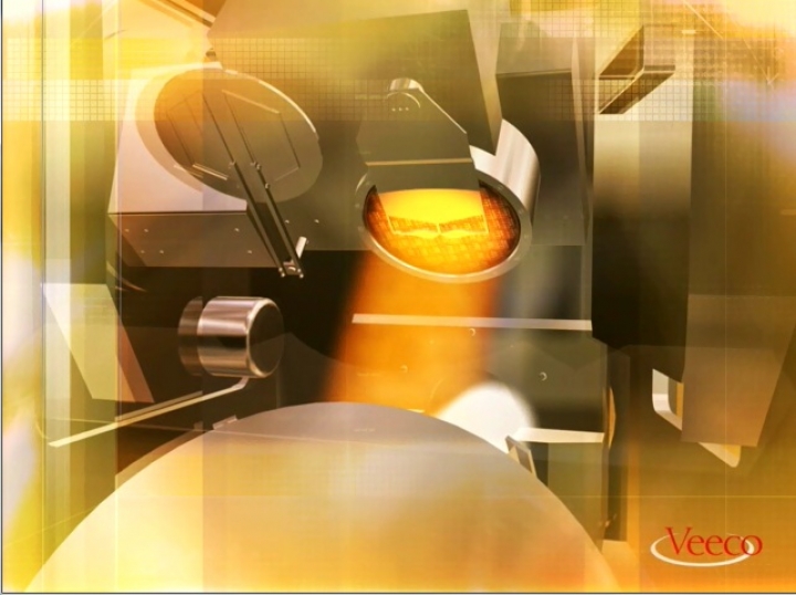
Ion beam deposition tools are used in the fabrication of EUV masks. The nanometre-scale patterns on masks are projected onto a semiconductor wafer to define a chip. A single mask may be used to print over 6 million chips during its life, requiring strict mask defect control.
Advanced-technology EUV masks are used to define chips with smaller geometries, which results in improved power and performance as required for an increasing number of mobile devices. Veeco says its IBD products enable high film quality, featuring extremely low particulate deposition and precise control of optical properties for single or multi-layer processes, two critical factors for producing advanced EUV photomasks.


