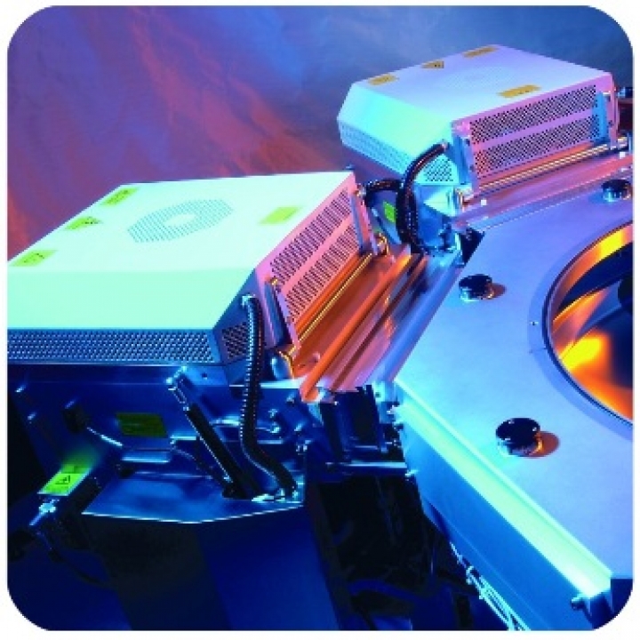
SPTS Takes On TSV 3D-IC Packaging Challenges

SPTS Technologies has developed a low temperature Plasma-Enhanced Chemical Vapour Deposition (PECVD) solution for via-reveal passivation in 3D-IC packaging applications.
Already used in 300mm volume production fabs, the Delta fxP PECVD system deposits dielectric layers onto bonded substrates at wafer temperatures below 200°C, with throughputs that the company says are up to twice that of its competitors.
Via reveal, or post-through silicon via (TSV) processing occurs after the TSVs are formed. Wafers are temporarily bonded, face -down to a carrier and then thinned from the back side to reveal the vias. The via tips are then passivated, typically with a combination of silicon nitride and oxide before final redistribution metallisation.
However, the temporary bonding adhesive introduces two challenges to the PECVD passivation step.
The first challenge is to deliver the required passivation film properties at a wafer temperature below 200°C to maintain the integrity of the temporary bond.
Second, the bonding adhesive will out-gas inside the PECVD vacuum chamber, disrupting the quality of the growing film. The Delta fxP cluster system provides unique solutions to these challenges.
SPTS has developed a number of hardware and process innovations to deposit low leakage current/high breakdown voltage TEOS oxides and nitrides at low wafer temperature. Excellent electrical isolation combined with high step coverage and mechanical robustness is obtained at a peak deposition temperature of less than 190°C. SPTS says its low temperature PECVD films are stable, with film properties staying constant over time.
To address the adhesive out-gassing problem, the Delta fxP carries an integrated batch Multi-Wafer Degas [MWD]. Since the temperature limit of bonded wafers is low, degas times of 15 minutes is not uncommon for some adhesives meaning significant cuts in productivity if a single wafer degas is adopted. By outgassing multiple wafers at the same time in the MWD, degas times up to 1 hour can be accommodated without compromising system throughput.
"SPTS possess a truly unique low temperature PECVD technology solution for via-reveal passivation," says Keith Buchanan, Marketing Manager for Advanced Deposition Products. "The combination of leading film properties and highest system throughput on bonded wafers addresses two of major obstacles in productionising post-TSV packaging."


