
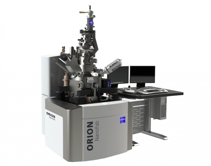
Carl Zeiss introduces ORION NanoFab
The new system extends nanofabrication of silicon semiconductors to the sub-10 nanometre scale and can be integrated with an FIB column
Carl Zeiss Microscopy is introducing ORION NanoFab at the European Microscopy Congress (EMC) in Manchester, UK.
The firm says it is the first multi-ion-beam tool based on Gas Field Ion Source (GFIS) technology.
As a major enhancement to the existing helium ion microscope, ORION NanoFab also utilises neon ions. The system is therefore capable of providing a complete sub-10 nanometre (nm) nanofabrication and sub-nanometre imaging solution for industry, government, and academic research laboratories. An optional gallium focused ion beam (FIB) column can also be integrated.
"This instrument offers sub-nanometre spatial resolution coupled with an extremely high depth of field, for the study of a wide variety of materials such as carbon based materials, co-polymers, and device structures, and also offers options for a variety of advanced microanalytical techniques," says Dr. David Joy, Distinguished Scientist at the Centre for Nanophase Materials Science (CNMS), Oak Ridge National Laboratory. CNMS at Oak Ridge National Laboratory (ORNL) is a Department of Energy / Office of Science Nanoscale Science Research Centre (NSRC).
The neon ion beam offers precise machining and nanofabrication capabilities due to higher sputter yields in ion beam milling and faster resist exposure in ion beam lithography. The helium ion beam allows sub-10 nm nanofabrication as well as high resolution imaging capability in the same instrument. The optional gallium FIB column allows massive material removal. Carl Zeiss says this makes ORION NanoFab one of the most versatile nanofabrication and imaging platforms available.
"I have finally found the system that I was looking for the past five years," says Dr. Qianjin Wang from the Physics Department at Nanjing University in China. "As a gallium FIB user for past ten years, I feel lucky that I will be at the forefront of revolution in the nanoworld as I focus on my research on optical properties of artificial nanoscale structures."
"We're very excited about all aspects of ORION NanoFab." adds Michael Phaneuf, President of Fibics Incorporated, a FIB/SEM applications development company established in Ottawa, Canada in 1997. "The evolution to this generation helium-neon-gallium tool is truly impressive. The possibilities for multi-scale nanofabrication combining all three beams are truly remarkable, and the applications involving high resolution imaging with helium and neon are only now beginning to be realised. We are eager to start applications development on this platform, and see where it leads."


