
Escalating Thin Wafer Market To Drive Temporary Bonding
The need for better memory, logic, power devices & image sensors will boost the need for semiconductor wafers thinner than 100µm
Almost three quarters of the total number of semiconductor wafers manufactured are expected to be thinned by 2017. It's no surprise then, that the temporary bonding market is expected to increase in the forseeable future.
This is according to Yole Développement's latest report, " Thin Wafers, Temporary Bonding Equipment & Materials Market."
Consumer applications will be the biggest driver for smaller, higher-performing, lower-cost device configurations for use in various applications, such as memory and wireless devices. These new configurations, in turn, are pushing demand for thin (under 100 µm) and ultra-thin (below 40µm) semiconductor wafers.
Reduced thickness wafers are much needed. In cell phones, packaged dies must be less than 1.2mm thick and this number shrinks to 1mm for smart phones.
What's more, wafer thinning is the most efficient approach used for heat dissipation in thermal management. And for 3D integration, thin wafers bring higher Through Si Via (TSV) density, as pitch and dimensions are contracting.
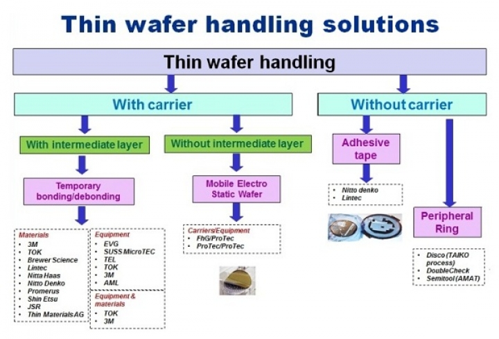
As you may expect, there are several manufacturing challenges the industry must confront as wafer thickness decreases to 100µm and below.
Ultra-thin wafers are less stable and more vulnerable to stress, and the die can be prone to breaking and warping - not only during grinding but also during subsequent processing steps.
Special thin wafer handling processes, or temporary bonding, is necessary, especially when wafers are dual-side processed or have high topographies.
Yole says this growing need for thin wafers is required for numerous applications. These markets include 3D ICs, MEMS, CMOS Image Sensors (CIS), Power Devices, LEDs, RF Devices, Memory & Logic, Interposers and Photovoltaic.

By 2017, the ratio of THIN wafers vs. TOTAL number of wafers (in 300 mm equivalent) will be 74 percent, corresponding to over 80 million 12'' or equivalent wafers , as depicted in the graph above.
The 2012 market drivers for thin wafers are 3D ICs, and also Power Devices and CIS BSI (backside illumination) for ultra-thin wafers. Indeed, the currently booming BSI application is the big driver for ultra thin wafers.
2011 was a big year for 300 mm wafer bonding tools, thanks to BSI. This application requires ultra thin layers of less than 10µm on 12'' wafers.
Yole anticipates that in 2017, most of the 12'' wafers will be 200µm thick for logic application and most of the thinned wafers will be in the 10-99µm thickness range. This includes memory, as well as interposers and power device applications.
Thin wafer handling will enjoy increased importance in the coming years, but as chips get thinner and wafer diameter increases, more complicated thinning/handling procedures will be required. This will intensify development in wafer thinning, wafer dicing and wafer temporary bonding.
Yole predicts that 10 percent of the total thin wafer shipment will experience a temporary bonding step by 2017. So, while temporary bonding equipment is currently a relatively small market, it is expected to grow as the need for thin wafer handling grows.
The market research firm actually estimates the market for temporary bonding tools to be more than $250 million by 2017. Currently, shipped bonder/debonders are for Power and 3D ICs applications. However, 3D ICs are perceived to become the predominant application for temporary bonders after 2015.
Temporary bonding requires know-how in process and chemistry, and an understanding of final application requirements. It is a complex technology, requiring an interface material (sometimes called the "Magic" material) that is strong enough to withstand post-processing but which can be easily removed afterwards.
The main concern for temporary bonding materials (wax, tape or glue) is temperature stability. Basically, the material must be strong enough to withstand processing steps (metallisation, etching, grinding).
Another issue is the choice of carrier material. The carrier lifetime of the material depends on its capability to withstand steps such as grinding and lapping, and carrier lifetime should be at least tens of times, though this is not the case at the moment.
So these hurdles must be overcome to enable the temporary bonding industry to move forward at the pace Yole believes is required.


