
Intel To Present 22nm Tri-Gate Technology For SoC Applications
Historically, gains in transistor performance have come from making them smaller. That has become more difficult and so innovations in transistor architecture are receiving more emphasis.
Multiple-gate transistors are one such innovation. They provide superior on/off control, enabling high drive currents to be achieved at a lower supply voltage than otherwise.
At the IEDM conference, Intel will discuss its use of the multiple-gate approach to build a complete and versatile 22-nm 3D tri-gate transistor technology platform for system-on-chip (SoC) applications.
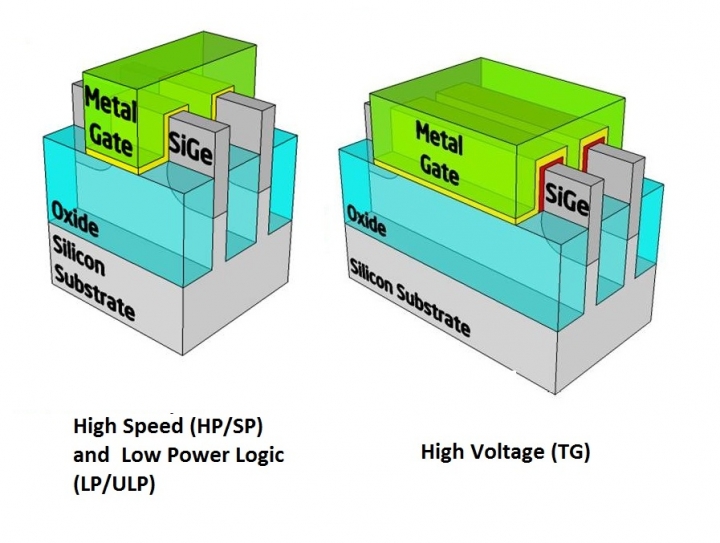
The image above shows 22nm SoC tri-gate transistor families, including high-speed logic, low power and high voltage.
Intel says the technology provides leading-edge transistors (families of high-speed, low-standby-power and high-voltage-tolerant devices), state-of-the-art interconnects and RF/mixed-signal features for a very wide range of SoC applications.
The high-speed logic transistors have sub-threshold leakages ranging from 100 nA/µm to 1 nA/µm, while the low-power versions feature leakage of less than 50 pA/µm yet have drive currents 50 percent higher than 32nm planar (traditional technology) devices. The process also yields high-voltage transistors (1.8 V or 3.3 V) for analogue circuits, I/O, legacy designs and other applications.
Intel says they feature the highest reported I/O device drive currents for an SoC technology (NMOS/PMOS = 0.92/0.8 mA/µm at 1.8 V). The trigate technology platform also features eight to 11 layers of low-k and ultra-low-k carbon-doped oxide (CDO) interconnect at tight pitches for different applications.
They feature many analogue/mixed-signal features and three different SRAM bit cells, spanning high-density/low-leakage (0.092 µm2), low voltage (0.108 µm2) and high-performance (0.130 µm2).
A presentation describing this work in greater depth, which will be presented at IEDM is, "A 22nm SoC Platform Technology Featuring 3-D Tri-Gate and High-k/Metal Gate, Optimised for Ultra-Low-Power, High-Performance and High-Density SoC Applications," by C.-H. Jan et al.
The 58th annual International Electron Devices Meeting (IEDM) will take place between December 10th and 12th, 2012 at the San Francisco Hilton Union Square, preceded by a full day of Short Courses on Sunday, December 9th and by a program of 90 minute afternoon tutorial sessions on Saturday, December 8th.

Fin cut TEM, gate cut TEM, and tilted SEM of logic thin gate (top) and high-voltage thick-gate (bottom) transistors

22nm modular transistor options and device characteristics


