
SPTS Joins 3D-IC 300mm Fraunhofer IZM ASSID Program
SPTS Technologies has signed a JDP Program with ASSID from Fraunhofer-IZM to research sub-1750C dielectric films in through silicon vias (TSV) for 3D-IC packaging.
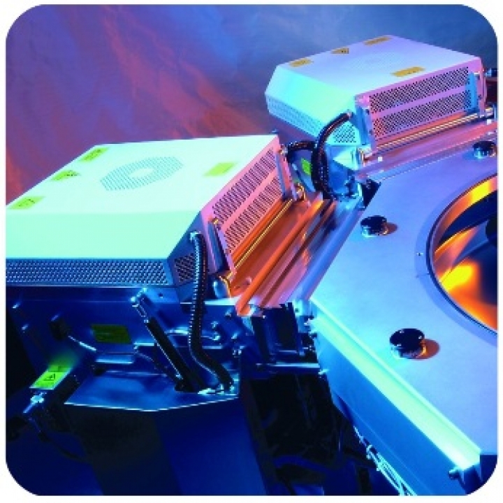
The program will use 300mm APM plasma enhanced chemical vapour deposition (PECVD) modules installed on a Versalis platform alongside SPTS etch chambers in the All Silicon System Integration Dresden (ASSID) centre in Dresden, Germany.
ASSID was set up in 2010, to develop 3D integration technologies on 300mm wafers, enabling leading device manufacturers to apply 3D-IC technology in volume production. By integrating the PECVD modules with etch processes on a single wafer handler, ASSID uses the Versalis system to optimise process results and reduce capital expenditure for development and pilot production.
The APM offers low temperature PECVD processes, targeting via-last TSV applications and via-reveal passivation. Dielectric layers for TSV isolation can be deposited at temperatures below 175°C to provide high sidewall coverage, low stress and proven "˜in-via' electrical performance.
For via-reveal, the APM offers high deposition rate silicon oxide and nitride films, compatible with silicon-on-glass substrates and combining excellent coverage, barrier properties and electrical isolation.
M. Juergen Wolf, the Manager of Fraunhofer IZM-ASSID and head of division HDI&WLP /ASSID says, "SPTS has been an important partner, who contributes valuable experience and production experience for our 300mm 3D device stacking assembly line. The additional PECVD capability provided another important process step in this line."
Kevin T. Crofton, executive vice president and chief operating office adds, "We're delighted to be a part of Fraunhofer's 300mm development line. SPTS is a leader in integrated 3D-IC solutions and we expect the advanced work Fraunhofer-IZM performed on our etch and PECVD process capabilities to accelerate the adoption of 3D packaging by volume manufacturers."
Delta PECVD Systems offer single-wafer processes for the deposition of dielectric films on wafer sizes up to 300mm. The PECVD chamber is supported by all SPTS cluster platforms and also by the unique Versalis fxP hybrid cluster system.
A single chamber design supports multiple wafer sizes. Digital control of critical hardware components provides a unique platen design enabling less than 200°C deposition temperatures. Key Delta applications include low temperature dielectrics for advanced packaging and tuned-stress films for MEMS.


