
Roth & Rau - Ortner To Reveal Customised Wafer Automation
The company plans to be more active in automation and expanding into electronics manufacturing. It hopes to eventually make the transition from 300mm to 450mm automation
Roth & Rau - Ortner is realigning its structure and expanding its industry expertise.
Previously, the company primarily focused on automation solutions for the semiconductor and photovoltaic industries.
"Effective immediately, we will also be more active in the growth industries for automation and expanding into electronics manufacturing, pharmaceuticals, and other high-tech industries," explains Heinz Martin Esser, CEO of Roth & Rau - Ortner GmbH.
"We will continue to focus on the semiconductor industry, yet we can transfer our products, solutions, and services in factory automation to other industries with complex requirements for automation," he adds. "Our branding with the new slogan 'Factory Automation Solutions' will show that we are clearly pursuing our core competences, while at the same time enabling us to polish up our established 'Ortner' brand. In this manner, we can remain successful on the market with a strong own identity."
Ortner is presenting "The Missing Link," which describes its custom designed automation solutions for existing semiconductor fabs to the public at SEMICONEuropa 2012.
These solutions are primarily directed at semi-automated production lines with high requirements for personnel. Older wafer fabrication businesses often called for the wafer to be handled manually between the production processes. It takes up valuable assets such as staff, causes high investments in time and cost, and is prone to error.
Now Ortner plans to develop automated customised solutions replacing formerly manual links between two work steps, including transportation, tool loading, storage and identification.
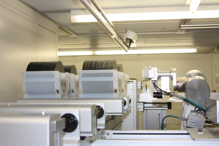
One of these automation projects has been implemented in a wet chemical process area of a major European semiconductor manufacturer that produces on 200mm wafers. The photo above shows a robot gripping a process carrier for 200mm automated tool loading .
"The offer has been well received on the market," comments Dr. Karli Hantzschmann, head of the Automation Business Unit. "We want to also greatly expand our new 'Automation' and 'Products' business areas in the near future to better serve our customers, in addition to expanding our traditionally strong 'Installation & Service' business area. We will be hiring new employees and start developing new products, too."
Ortner is a co-founder of the 450mm working group in Silicon Saxony e.V., an association for the high-tech industry in Germany.
"Transitioning from 300- to 450mm wafers poses a great challenge for chip manufacturers. Against this backdrop, we are investigating solutions for this technology. We are carefully studying all major programs and initiatives and are in close contact with IMEC Belgium and CSNE in the U.S.," says Esser. "Furthermore, we are members of the Dresden Fab Automation Cluster, Silicon Saxony e.V., and SEMI. We are committed to and closely cooperate with this strong network of partners."


