
Jenoptik packaging technology supports up to 300mm wafers
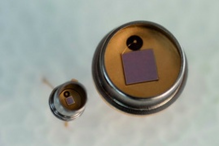
Jenoptik has developed a new product range of photodiodes with an angle-independent response spectrum.
Compared with conventional silicon photodiodes, the new photodiodes detect a predefined wavelength range without the need for the insertion of an additional filter.
The photodiodes are made from SiC and III-V semiconductors and are designed for a spectral range of 150 to 1750nm.
Unlike dielectric filters, they also provide spectral receiving characteristics that are independent of the angle of incidence of the radiation.
The new photodiodes are ideally suited for all photometric applications where an extended measurement range is required.
These new diodes can save space and follow the trend towards miniaturisation while simplifying assembly.
Jenoptik provides customer specific solutions and a wide range of photodiode products as preassembled standard products in SMD and TO housings.
Their detection is wavelength-selective. Jenoptik says they have very good signal and noise performance. In hermetically sealed special housings, they are thermally stable up to 125°C.
Photodiodes provide safety.
They are widely-used in the automotive, security and health care industries in a wide range of applications. These include daylight/tunnel sensors or lane departure warning systems in vehicles.
They can be applied in monitoring safety levels in gas detectors, in water disinfection of UV radiation, as flame sensors for burner monitoring, as detectors in photoelectric sensors, and for analysis of body fluids concentration in medical technology.
Jenoptik has extended its assembly and packaging process chain by recent investments in wafer sawing and multi-chip bonding, and can processe wafers of up to 300mm.
This enables customers to realise economical solutions with high-precision production processes that are at the forefront of technology.
The new systems are particularly suitable for the processing of complex customised micro-electronic components such as image processing sensors.
Using the more powerful double-spindle wafer saw, the new fully automatic system cuts, cleans and exposes the wafers contained in a magazine.
Jenoptik says the two-spindle saw also reduces the cycle time by more than half when compared to semi-automatic processes.
Its intelligent water supply system makes the saw especially suitable for the processing of silicon-based image sensors and optical glass.
Jenoptik is now working with a multi-chip bonder to further process the 300mm wafers.
Depending on the quality of the source material, this chip bonder achieves a placement accuracy of up to ±10 µm and can process chips with an edge length of between 0.2 and 80mm.
The main advantage of 300mm wafer source material is that there is less waste.
Depending on the chip size required, there is a correspondingly higher yield per wafer. This substantially reduces manufacturing costs for semiconductor chips in comparison with smaller wafer diameters.


