
Alpha and Omega Semiconductor XS MOSFETs Raise The Bar In Packaging
Four new devices from the firm are t suited to telecom, data storage and motor control applications
Alpha and Omega Semiconductor Limited (AOS) believes it has set a new standard in power density and technology innovation for discrete power MOSFETs.
The new exposed-source XSFET, is a new type of packaging technology, which is patent-pending.
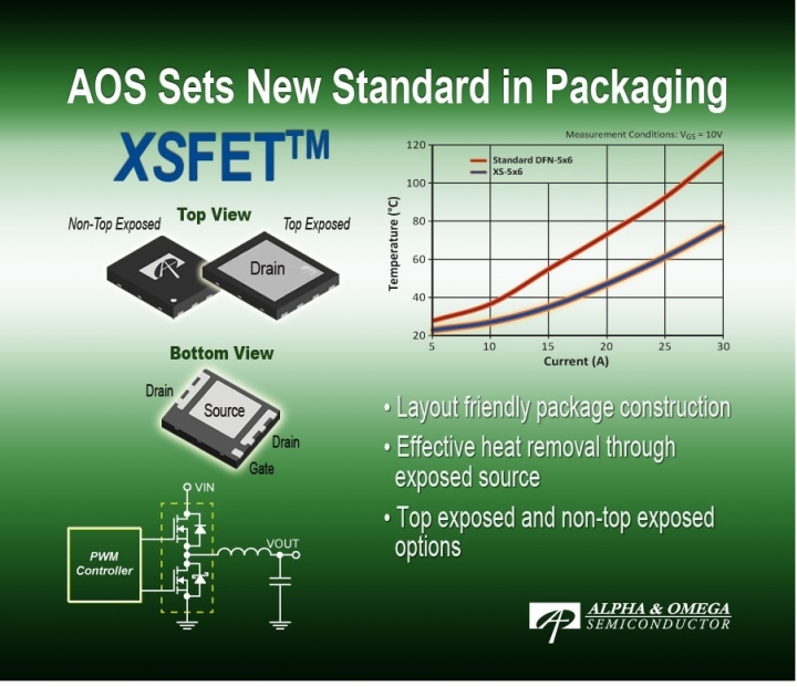
XSFET incorporates the packaging technology where the bottom of the package is the "source." This enables power designers to remove heat more effectively to PCB ground plane. It features a large top heat slug which can be "top-exposed" or "non top-exposed" depending upon design criteria.
The top-exposed version delivers a significant increase in heat transfer, which helps to reduce power losses in a system by keeping the die cooler.
Distinct from some of the existing double-sided cooling packaging options on the market today, AOS's new exposed-source packaging solution offers standard lead-frame based board mounting in a fully encapsulated DFN molded package. AOS says it minimises the thermal discrepancy between the device and the PCB while offering near zero parasitic inductance with its layout friendly footprint.
Employing AOS's new 30V AlphaMOS silicon technology together with exposed-source packaging, AOE6580 and AOE6580T (with top-exposed option) are claimed to be the best-in-class 30V N-channel devices on the market today.
Both devices are optimised for high performance demanding motor control, OR'ing, and E-fuse applications. Their very low on-resistance (RDS(ON) = 0.95mΩ max @10VGS) in exposed-source DFN 5 x 6 package also make these devices very attractive for power supplies in computing, telecom, and high power density point-of-load sockets.
Optimised for ultra-low conduction and switching losses, both the AOE6580 and AOE6580T minimise power losses in applications, and provide power designers the flexibility, performance, space, and cost.
The AOE6770T and AOE6772T offer high efficiency in server and high-end notebook applications by using a combination of 25V AlphaMOS silicon technology and exposed-source packaging technology with the top-exposed option in industry standard DFN5x6 footprint. AOE7770T completes the solution as high-side MOSFET by combining exposed-source technology in compact DFN3x3 footprint with top-exposed option.
"AOS's new XSFET packaging technology sets a new Industry standard for higher power density and performance. Our new devices with both "top-exposed" and "non top-exposed" versions enable power designers to reduce power losses and increase performance significantly," says Yalcin Bulut, Vice President of Discrete Product Lines at AOS.
"The exposed-source technology allows electronic designs to achieve higher current density while keeping components operating cooler. AOS tailored its technology to lead in innovation for solutions which make a difference in today's demanding application requirements."
AOE6770T, AOE6772T, AOE7770T, AOE6580, and AOE6580T are in halogen-free DFN packages and are MSL1 rated.


