
First EUV lithography optics from Carl Zeiss
The "Lithography for the 22 nanometre node" project, led by Carl Zeiss, has been successfully completed.
The national project was part of the European EXEPT Project ("Extreme UV Lithography Entry Point Technology Development") led by the Dutch company ASML, as part of the CATRENE Cluster.
During the project, two Carl Zeiss companies and six other German companies and research facilities developed EUV lithography. They started at a basic research stage and migrated to a technology which can be fully implemented for the volume production of microchips on the 22nm node.
Through EUV technology, Carl Zeiss and its partners are trying to enable smaller, more efficient, environmentally friendly and affordable microchips. The project was supported by the German Federal Ministry for Education and Research (BMBF) to the tune of approximately Euros (€)16 million in total.
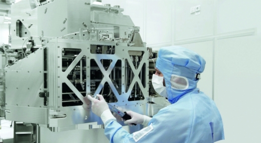
EUV is an optical lithography procedure which uses extreme ultraviolet light to transfer integrated circuits to microchips. The production of a demonstrator of a first EUV projection system marked the attainment of one of the key project goals of Carl Zeiss SMT GmbH.
The foundation was hence laid for supplying strategic partner ASML with key components of the EUV scanner in the future. "The successful collaboration for the further development of this crucial technology helped further strengthen the leading role of German companies in the area of microelectronics," sums up Hermann Gerlinger, Member of the Executive Board of Carl Zeiss AG and CEO of Carl Zeiss. "We support the German site. Targeted support, like that from BMBF, supports us in expanding the necessary competencies."
Within the scope of the project, the partners had developed the projection system required for the lithography process, together with the necessary infrastructure.
The contributions of Carl Zeiss SMT GmbH centre in Oberkochen was effective in a number of ways. The firm managed to incorporate a more powerful projection lens, a highly flexible illumination system without loss of energy, and the high-accuracy measuring systems necessary for qualification.
IMS Chips, based in Stuttgart, supplied new optical elements for the precision measurement of the EUV mirror. Carl Zeiss SMS GmbH in Jena, Rossdorf, developed mask repair processes for EUV photo masks. This was supported by the Fraunhofer Institute for Integrated Systems and Device Technology based in FhG IISB, Erlangen, in carrying out theoretical experiments using special EUV simulation software.
Bruker ASC GmbH in Cologne developed EUV/XUV-based metrology solutions which can be used in reflectometers for the optical characterisation of EUV masks, among other applications.
SÜSS MicroTec Photomask Equipment GmbH & Co. KG, based in Sternenfels, provided process facilities and processes for the cleaning and automated handling of the EUV masks, while Dynamic Microsystems GmbH (DMS, Radolfzell) provided facilities for the cleaning and decontamination of the EUV mask transport containers.
The facilities and processes supplied by these two companies fulfil very high cleanliness specifications. The Advanced Mask Technology Centre GmbH & Co. KG in Dresden, Germany developed appropriate cleaning technologies for 20nm technology EUV masks.
The project has also started to bear fruit from a commercial viewpoint.
Alongside Carl Zeiss, SÜSS MicroTec and DMS managed to supply the first demonstrators and technologies developed within the scope of the project to customers around the world. Thus, each of these companies has managed to carve out a place for itself in technology leadership and a significant position on the market.
Through EUV lithography, Carl Zeiss strives to adhere to Moore's law, which says that integrated circuits on microchips double approximately every 18 months.
EUV enables the further miniaturisation of integrated circuits, which significantly increases the performance of the microchips.


