
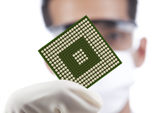
Nanoelectronics could aid computer chip designers
To build the computer chips of the future, designers will need to understand how an electrical charge behaves when it is confined to metal wires only a few atom-widths in diameter.
Now, a team of physicists at McGill University, in collaboration with General Motors R&D, have shown that electrical current may be drastically reduced when wires from two dissimilar metals meet.
The surprisingly sharp reduction in current reveals a significant challenge that could shape material choices and device design in the emerging field of nanoelectronics.
The size of features in electronic circuits is shrinking every year, thanks to the aggressive miniaturisation prescribed by Moore's Law. The theory postulates that the density of transistors on ICs would double about every 18 months.
This steady progress makes it possible to carry around computers in our pockets, but poses serious challenges.
As feature sizes dwindle to the level of atoms, the resistance to current no longer increases at a consistent rate as devices shrink; instead the resistance "jumps around," displaying the counterintuitive effects of quantum mechanics, says McGill Physics professor Peter Gruetter.
"You could use the analogy of a water hose," Gruetter explains. "If you keep the water pressure constant, less water comes out as you reduce the diameter of the hose. But if you were to shrink the hose to the size of a straw just two or three atoms in diameter, the outflow would no longer decline at a rate proportional to the hose cross-sectional area; it would vary in a quantised ('jumpy') way."
This "quantum weirdness" is exactly what the McGill and General Motors researchers observed, as described in a paper appearing in Proceedings of the National Academy of Sciences. The researchers investigated an ultra-small contact between gold and tungsten, two metals currently used in combination in computer chips to connect different functional components of a device.
On the experimental side of the research, Gruetter's lab used advanced microscopy techniques to image a tungsten probe and gold surface with atomic precision, and to bring them together mechanically in a precisely-controlled manner.
The electrical current through the resulting contact was much lower than expected. Mechanical modelling of the atomic structure of this contact was done in collaboration with Yue Qi, a research scientist with the General Motors R&D Centre in Warren, Michigan.
State-of-the-art electrical modelling by Jesse Maassen in professor Hong Guo's McGill Physics research group confirmed this result, showing that dissimilarities in electronic structure between the two metals leads to a fourfold decrease in current flow, even for a perfect interface.
The researchers also found that crystal defects generated by bringing the two materials into mechanical contact, was a further reason for the observed reduction of the current.
"The size of that drop is far greater than most experts would expect -on the order of 10 times greater," notes Gruetter.
The results point to a need for future research into ways to surmount this challenge, possibly through choice of materials or other processing techniques. "The first step toward finding a solution is being aware of the problem," Gruetter adds. "This is the first time that it has been demonstrated that this is a major problem" for nanoelectronic systems."
Funding for this research was provided by the Natural Sciences and Engineering Research Council of Canada, le Fonds Québécois de la Recherche sur la Nature et les Technologies, and the Canadian Institute for Advanced Research.


