
FEI's Helios NanoLab 450 F1 Aids Semiconductor Failure Analysis
FEI is introducing its new Helios NanoLab 450 F1 DualBeam system designed to provide semiconductor manufacturers with faster, better images of their most advanced device architectures.
A new STEM (scanning transmission electron microscope) detector delivers improved contrast between materials, and the new flip stage and rotating nanomanipulator support advanced preparation techniques for complex device architectures. These include finFETs and 3D memory structures.
Ultimately, faster, better answers cut development costs, accelerate process ramps, and get new products to market sooner.
"The F1 combines our best new technologies into an industry leading DualBeam for semiconductor failure analysis," says Rudy Kellner, vice president and general manager of FEI's Electronics Business Unit.
"The new STEM detector lets the operator know precisely when the sample is thin enough, and in many cases, the images can eliminate the need for standalone TEM analysis altogether. In fact, as samples get thinner there are advantages to working at lower beam energies where interactions with the sample are stronger. The new EasyLift nanomanipulator and flip stage let the operator manoeuvre the sample quickly and easily for inverted thinning, to monitor end-pointing from both sides of a section, or to section a 3D device at almost any angle."
Dual beam instruments combine an SEM (scanning electron microscope) for imaging and a FIB (focused ion beam) for milling and deposition. Such systems also provide STEM imaging capability by adding a detector for collecting transmitted electrons below the sample.
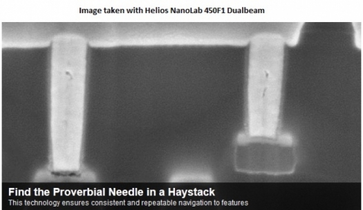
An increasingly important application of dual beam instruments is the preparation of the ultra thin samples required for TEM analysis. This need for high-resolution TEM analysis has grown dramatically in recent years as many devices structures have shrunk beyond the resolving power of SEM.
The Helios NanoLab 450 F1 is the most recent addition to FEI's line of DualBeam systems.
It combines the industry's highest resolution SEM and FIB for high quality imaging and fast, precise milling and deposition, and adds capabilities specifically designed for semiconductor failure analysis applications. The new STEM detector delivers higher resolution and better material contrast.
The FlipStage 3 quickly flips the sample between thinning and STEM viewing positions and a new rotation axis permits viewing from either side of the section. The EasyLift nanomanipulator provides precise motorised sample manipulation, including rotation, to support automated "lift-out" and advanced preparation procedures, such as inverted thinning. The MultiChem gas injector system provides unprecedented flexibility in gas assisted milling and deposition, while also cutting maintenance costs with pre-filled crucibles.


