
Yole: Wireless To Drive Embedded Wafer Level Packaging
After Infineon's strong push for eWLB technology commercialisation and the resulting surge in growth, the Fan Out Wafer Level Packaging (FOWLP) market reached the $100 million market last year.
Revenue is now stabilising as Intel Mobile will progressively phase out its key wireless baseband SoC product production, outsourced currently at packaging subcontractors, Taiwanese ASE, Portuguese firm, NANIUM and STATS ChipPAC, based in Singapore.
This young industry will need to wait until 2015 to 2016 to reach $200 million, as the demand will shift from IDMs to leading fabless wireless IC players, such as Qualcomm, Broadcom and Mediatek, and will be supported by the solid infrastructure of "˜top 4' major assembly houses.
Yole has examined the subject in depth and is releasing a report detailing its findings in the publication, "ADVANCED PACKAGING : FOWLP & Embedded Die Packages," on 20th November.
Low reliability on large package body size and lack of flexibility in the IC to package co-design process are the two main factors limiting the wide adoption of FOWLP technology in the wireless IC market.
Indeed, FOWLP technology imposes a specific redesign of the chip for efficient integration into the package. Both Infineon and STEricsson (who already have products on the market) spent almost 18 month to redesign their baseband and RF-Transceiver SOCs in order to place the pads at optimised locations and match with a single RDL, 0.5mm board pitch eWLB package design.
FOWLP is a restrictive package technology for most of the world's IC designers to adopt efficiently, especially fabless chip companies. This is why only big semiconductor IDM companies having IC-to-package co-design environments well established in-house can drive and support the initial growth of this new wafer-level-packaging platform at its early stages.
According to Yole, FOWLP is clearly the "middle-end" platform of choice for packaging assembly & test "˜OSAT' suppliers of the IC industry, as all implies a simplification and consolidation of the entire packaging, assembly & test and supply chain inside one single factory.
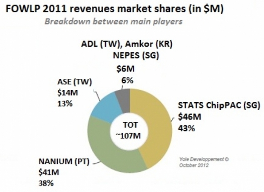
NANIUM and STATS ChipPAC shared more than 80 percent of the $107 million FOWLP activity revenue last year, mainly driven by Intel Mobile's volume demand on eWLB production.
While ASE is shutting down its 200mm eWLB operations this year to focus on future generation FOWLP technologies, many OSAT players are presently in the qualification phase such as ADL from Taiwan, Korean Amkor and Singapore based NEPES.
Additional packaging houses are expected to come onboard in the 2013 "“ 2014 time frame such as Taiwanese firms TSMC and SPIL and Japanese company, J-Devices.
Meanwhile, the embedded die in package industry took a giant leap forward in 2011 since Austrian firm AT&S and US based TI, started the commercialisation of microSiP DC/DC converter modules with critical mass volume, production of over 100 million units this year, driven by the mobile market.Rohm, and Epcos-TDK, both from Japan, would be the second source of the same microSiP power conversion module in the mobile handset supply chain of RIM, based in Canada.
Japanese IC substrate suppliers Taiyo-Yuden and Fujikura are also getting set to ramp-up their internal assembly lines for embedded die packaging. This will bring the total number of players to 4 in the near future, with separate supply chains able to support the embedded die in package technology commercialisation.
Today, the main roadblocks for embedded die package commercialisation are mainly linked to low manufacturing yields (75-85 percent overall) and supply chain settlement issues in both the embedded die wafer preparation as well as in back-end assembly & test operations.
Again, only a large semiconductor IDM company such as Texas Instruments (TI) could successfully lead the commercialisation of this new packaging assembly platform by filling the gaps (in terms of investment, risk and know-how) and settle the supply chain.

The most pragmatic approach to commercialise embedded die package technology will be to initially start with simple, low cost, low I/Os, small die analogue & power IC applications (such as DC/DC converter modules, IPD networks, RFID, Power MOSFET, IGBT modules, auto-focus driver ICs, etc"¦)
Embedded die packaging is supported by a game changing, low cost, panel area, PCB based infrastructure that has the potential to create a new space, an alternative supply chain for today's well established package standards such as QFN/SOT/WLCSP/BGA platforms. Being intrinsically "3D" capable, the technology is well positioned to meet the future requirements of miniaturised, low cost 3D SiP module configurations.
Today, first generation's of FOWLP and embedded die package technologies are not really competing as they are driven by different players and will initially target very different application spaces. However, this situation is likely to change radically in the near future as "2nd generation" derivatives of both platforms appear on the market.


