Lithography & Wafer Fab Projects Awarded By 2012 ENIAC JU

The IMPROVE project, which focuses on wafer fab efficiency and LENS, which targets the lithography supply chain have been honoured for innovation
Two research projects with a combined budget approaching 70 million Euros achieved significant advances in semiconductor manufacturing efficiency and have been recognised with the 2012 ENIAC JU INNOVATION AWARD at the European Nanoelectronics Forum.
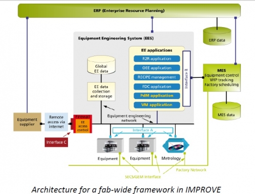
The IMPROVE project partners developed computational models for equipment behaviour and history enabling virtual metrology, predictive maintenance and adaptive control plans to considerably improve throughput, stability and reproducibility, and the overall wafer fab efficiency.
Francois Finck of STMicroelectronics, the project coordinator, says, " In IMPROVE, six manufacturers with operations in Europe collaborated with 14 research laboratories, institutional and academic, and 10 industrial solution providers to considerably advance the state of the art in manufacturing sciences and get ready to compete based on efficiency and innovation".
In LENS, 12 partners considerably advanced design, masks, metrology, exposure tool, materials and process integration using double exposure for systems on chip and spacer based pitch doubling for phase change memories to extend the applicability of the incumbent immersion lithography technology.
Gerold Alberga of ASML, the project coordinator, adds, "LENS covered the whole lithography supply chain, demonstrating patterning resolutions compatible with the 32 - 22nm technology nodes for both memory and logic devices using immersion exposure tools, thereby allowing the timely and economically efficient development of the next generations of semiconductor devices".
The projects received grants from the ENIAC JU and the ENIAC member States (IMPROVE: Austria, France, Germany, Ireland, Italy and Portugal; LENS: Belgium, France, Italy, Spain and The Netherlands).
Andreas Wild, ENIAC JU Executive Director, continues, "IMPROVE and LENS have been selected in the open and competitive call for proposals from 2008, and came to completion this year. Between 2008 and 2011, the ENIAC JU programme launched 40 projects with combined budgets exceeding 1 billion Euros (€), confirming the sizable impact that public-private partnerships have on sparking innovation."
The ENIAC Joint Undertaking (JU) is a public-private partnership on nanoelectronics bringing together the ENIAC member States, the European Union, and AENEAS (an association representing European R&D actors in this field).
It coordinates research activities through competitive calls for proposals to enhance the further integration and miniaturisation of devices, and increase their functionalities. It aims to deliver new materials, equipment and processes, new architectures, innovative manufacturing processes, disruptive design methodologies, new packaging and "˜systemising' methods, driving and been driven by innovative high-tech applications in communication, computing, transport, health care, wellness, energy, environmental management, security and safety, and entertainment.
Set up in February 2008, the ENIAC JU will allocate grants throughout 2013. The projects selected for funding shall be executed till 31st December 2017. The total value of the R&D activities generated through ENIAC JU is estimated at €3 billion.


