
Cadmium Selenide Competes With Amorphous Silicon
Electronic circuits are typically integrated in rigid silicon wafers, but flexibility opens up a wide range of applications.
In a world where electronics are becoming more pervasive, flexibility is a highly desirable trait, but finding materials with the right mix of performance and manufacturing cost remains a challenge.
Now a team of researchers from the University of Pennsylvania has claimed that nanoscale particles, or nanocrystals, of the semiconductor cadmium selenide (CdSe) can be "printed" or "coated" on flexible plastics to form high-performance electronics.
The research was led by David Kim, in the Department of Materials Science and Engineering in Penn's School of Engineering and Applied Science and the work was published in the journal Nature Communications.
"We have a performance benchmark in amorphous silicon, which is the material that runs the display in your laptop, among other devices," Kagan, a co-author of the publication, says. "Here, we show that these cadmium selenide nanocrystal devices can move electrons 22 times faster than in amorphous silicon."
Besides speed, another advantage cadmium selenide nanocrystals have over amorphous silicon is the temperature at which they are deposited.
While amorphous silicon uses a process that operates at several hundred degrees, CdSe nanocrystals can be deposited at room temperature and annealed at mild temperatures, opening up the possibility of using more flexible plastic foundations.
Another innovation that allowed the researchers to use flexible plastic was their choice of ligands, the chemical chains that extend from the nanocrystals' surfaces and helps facilitate conductivity as they are packed together into a film.
"There have been a lot of electron transport studies on cadmium selenide, but until recently we haven't been able to get good performance out of them," Kim says. "The new aspect of our research was that we used ligands that we can translate very easily onto the flexible plastic; other ligands are so caustic that the plastic actually melts."
Because the nanocrystals are dispersed in an ink-like liquid, multiple types of deposition techniques can be used to make circuits. In their study, the researchers used spincoating, where centrifugal force pulls a thin layer of the solution over a surface, but the nanocrystals could be applied through dipping, spraying or ink-jet printing as well.
On a flexible plastic sheet a bottom layer of electrodes was patterned using a shadow mask, essentially a stencil, to mark off one level of the circuit. The researchers then used the stencil to define small regions of conducting gold to make the electrical connections to upper levels that would form the circuit.
An insulating aluminium oxide layer was introduced and a 30nm layer of nanocrystals was coated from solution. Finally, electrodes on the top level were deposited through shadow masks to ultimately form the circuits.
"The more complex circuits are like buildings with multiple floors," Kagan says. "The gold acts like staircases that the electrons can use to travel between those floors."
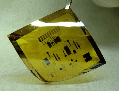
The image above shows the flexible circuit fabricated in the Kagan lab. (Photo courtesy of David Kim and Yuming Lai).
Using this process, the researchers built three kinds of circuits to test the nanocrystals performance for circuit applications: an inverter, an amplifier and a ring oscillator.
"An inverter is the fundamental building block for more complex circuits," Lai, another co-author of the paper, comments. "We can also show amplifiers, which amplify the signal amplitude in analogue circuits, and ring oscillators, where "˜on' and "˜off' signals are properly propagating over multiple stages in digital circuits."
"And all of these circuits operate with a couple of volts," Kagan says. "If you want electronics for portable devices that are going to work with batteries, they have to operate at low voltage or they won't be useful."
With the combination of flexibility, relatively simple fabrication processes and low power requirements, these cadmium selenide nanocrystal circuits could pave the way for new kinds of devices and pervasive sensors, which could have biomedical or security applications.
"This research also opens up the possibility of using other kinds of nanocrystals, as we've shown the materials aspect is not a limitation anymore," Kim points out.
More details of this work can be accessed in the paper, "Flexible and low-voltage integrated circuits constructed from high-performance nanocrystal transistors," by David K. Kim et al in Nature Communications, 3, Article number 1216,. DOI: 10.1038/ncomms2218
The research was supported by the U.S. Department of Energy and the National Science Foundation.


