
Carl Zeiss extends metrology systems for EUV lithography with PTB
Carl Zeiss and the German national metrology institute Physikalisch Technische Bundesanstalt (PTB) will be expanding their cooperation in the future.
This is to advance optics metrology for EUV (extreme ultraviolet) lithography of semiconductors.
The two institutions have signed a cooperation agreement for a further four years.
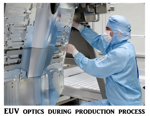
Along with its Dutch partner ASML, Carl Zeiss is working on the development of EUV lithography, an innovative technology for generating integrated circuits on wafers using a wavelength of 13.5 nm.
The lithography optics from Carl Zeiss are integrated in a wafer scanner at the facilities of the global market leader ASML. The PTB supports Carl Zeiss with high-precision measurements of EUV optical components using a new EUV beamline at the PTB's very own electron storage ring, the Metrology Light Source.
The PTB and Carl Zeiss have been working together since 1998.


