
KLA-Tencor launches MEMS wafer inspector
The ICOS WI-2280 system is designed to provide manufacturers with greater flexibility, reduced cost of ownership and improved efficiency
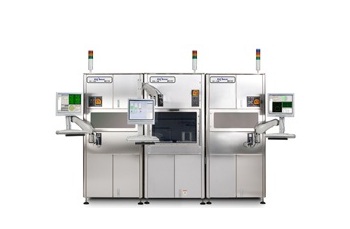
KLA-Tencor Corporation has revealed its next-generation wafer inspection tool, the ICOS WI-2280.
The tool is designed specifically for defect inspection and 2D metrology for LED applications.
But the ICOS WI-2280 also provides enhanced inspection capabilities and increased flexibility for microelectromechanical systems (MEMS) and semiconductor wafers spanning two inches to eight inches in size.
The ICOS WI-2280 is KLA' fourth generation wafer inspection system and is built on its WI-22xx platform, delivering sensitivity with increased throughput.
What's more, the tool supports handling of whole wafers in carriers and diced wafers in hoop ring or film frame carriers to accommodate multiple media with minimal equipment changeover time.
The WI-2280 also features an enhanced rule-based binning defect classification and recipe qualification engine, enabling manufacturers to achieve faster yield learning during production ramps, as well as improve process control and process tool monitoring strategies in their manufacturing process.
The ICOS WI-2280 includes flexible advanced optical modes with dedicated image processing. This enables a high defect capture rate and recipe robustness against varying process backgrounds.
The tool can also classify defects uniquely and has an advanced recipe tuning engine and enhanced metrology capability.
Front-end to back-end-of-line connectivity analysis is also possible, delivering a single platform for defect source analysis. KLA says the system has an easy-to-use inline or offline reclassification engine. This enables post-inspection yield improvements for enhanced productivity
The MEMS semiconductor market can leverage the ICOS WI-2280 tool for back-end-of-line and post-dicing outgoing quality control or binning; front-end-of-line patterned wafer inspection for baseline yield improvement, rework, excursion control or overlay; and 2D surface inspection and metrology.


